How long until xfade is ready? Maybe I should pay for blur now and wait for delivery until xfade is ready, don’t want to miss out on blur
1 Like
1x PCB set for me please
Thank you!
2 Likes
the xfade is ready, just have to determine the price and make some pictures
3 Likes
Would love two built modules, thanks! I’m in California
2 Likes
1 full kit, please. Located in Vienna.
2 Likes
The parts came in today, I’ll start building tomorrow
3 Likes
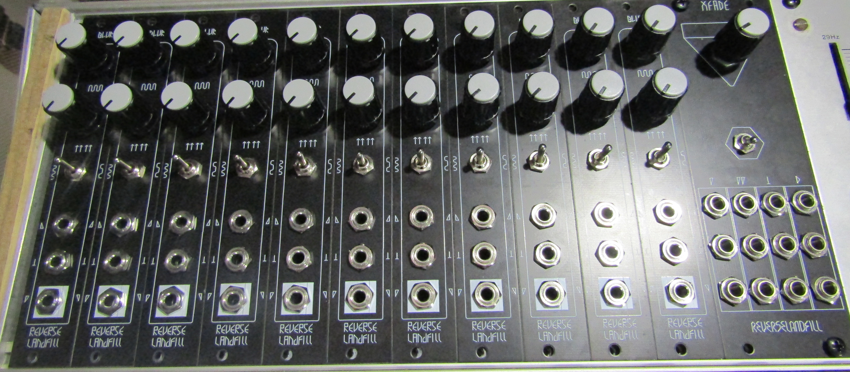
Building 9 modules progress: all resistors, diodes, ferrites done. tomorrow I’ll continue ![]()
5 Likes
BOM updated again ![]() I forgot the 78L05
I forgot the 78L05
module builds will be mostly finished today, I’ll contact all people on the list then
2 Likes
13 Likes
patch them all in series, blur the blurring the blur
2 Likes
Not sure if this is the right thread (or forum?) for support questions, but I’m working on gathering components for this, and I found a discrepancy between the build guide and the BOM/schematic so now I’m a little confused and want to make sure I’ll put the right components.
The BOM (v3f-2) lists the following 3 filter value capacitors:
| designator | value | details |
|---|---|---|
| c10 | 220pF-470pF | 5mm film, filter value1 |
| c9 | 820pF-2.2nF | 5mm film, filter value2 |
| c8 | 8.8nF-12nF | 5mm film, filter value3 |
And the schematic (v3d-1) shows these values for these capacitors:
c8 = 10nF
c9 = 1nF
c10 = 470pF
(which fits in the ranges specified in the BOM)
But the build guide (v1-1) mentions the following about these capacitors:
C8: 470pF, C9: 1nF and C10: 10nF
(which has C8 and C10 switched when comparing to the BOM/schematic)
I’m not sure if the order matters for the switch circuity (I should be able to reason it out, but it was a draining day at work so my brain isn’t the freshest right now), so I wanted to check to see which is preferred or correct, if the order matters.
2 Likes
Hey Joem, I looked at the schematic and C10 is connected to the common pin of the switch so I believe that one should be the smallest value (470pF).
It definitely wouldn’t hurt to @ @reverselandfill just to be 100%.
3 Likes
Fixed!. Thanks for spotting this!
updated BOM & Guide 10-08-22
the guide has new pictures added (switch soldering and jack tabs explained)
Note: On the panel, the jack holes and the potmeter holes are not in the same horizontal position.
This is to correct the height difference of the jacks comparated to the potmeters
(about 1 / 1.5 mm)
2 Likes
I’d like to get 2x PCB/Panels. Are there still some available, @reverselandfill?
1 Like
Kent 1x kit shipped
Hewed: 2x pcb panel - shipped
1 Like
Hey man,
2 x pcb and panel for me if there are still any left.
Cheers
I’d love a built one if they’re still up for grabs. I’m in Thailand and have had stuff shipped here before so it’s doable. Cheers!
The first batch is all gone,
I’ll order new pcbs and post here when they are available again!
7 Likes
Sweet cheers man. Much appreciated
New pcbs will arrive at the end of this week
2 Likes