Late to the party here. I think this is a great idea! Have tinkered with a kind of plugin header for my own breadboarding, but it didnt fell out that good…
One thing i would like added is a few toggle switch headers, since these are always a PIA to fit on breadboards. Preferably 2 standard SPDT, and one DPDT. And if people dont need those in their designs, they can leave them not soldered
I will have to make a big manual for this project, with all possibilities packed in like this.
Already I can see an update with a more systematic layout / graphics on top of it all.
I’m not fond of so much text on the pcb. maybe I’ll do something about this…
fast delivery costs more, but I like fast
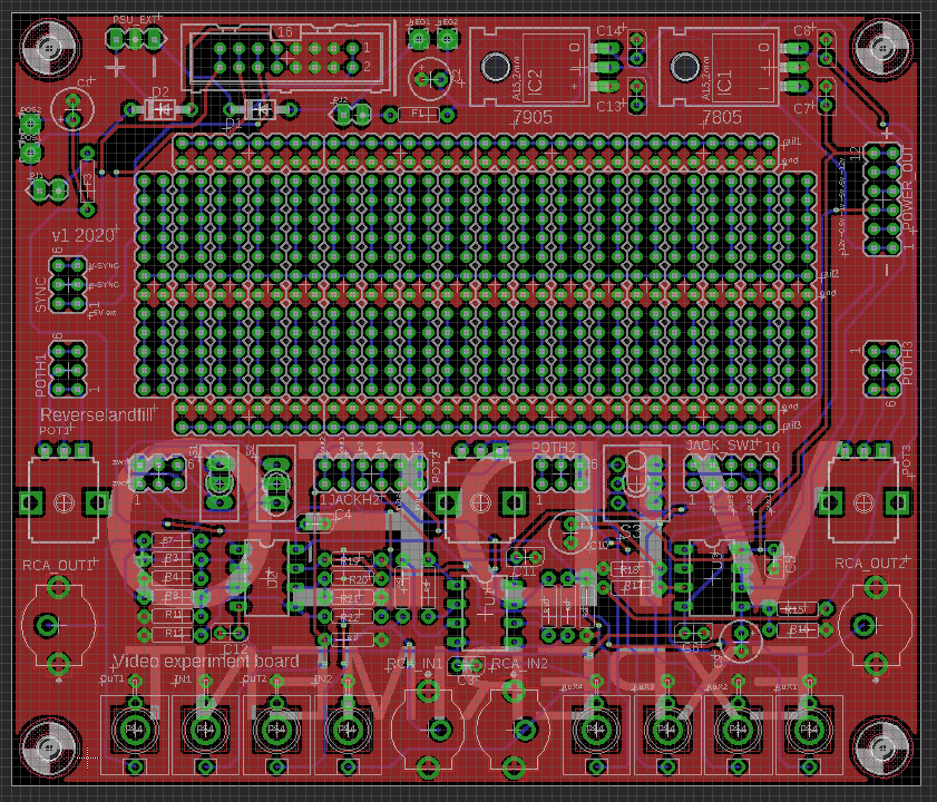
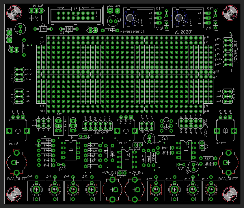
the only mistakes I can see for now is that I forgot the middle rails markings. but that is not really a problem.
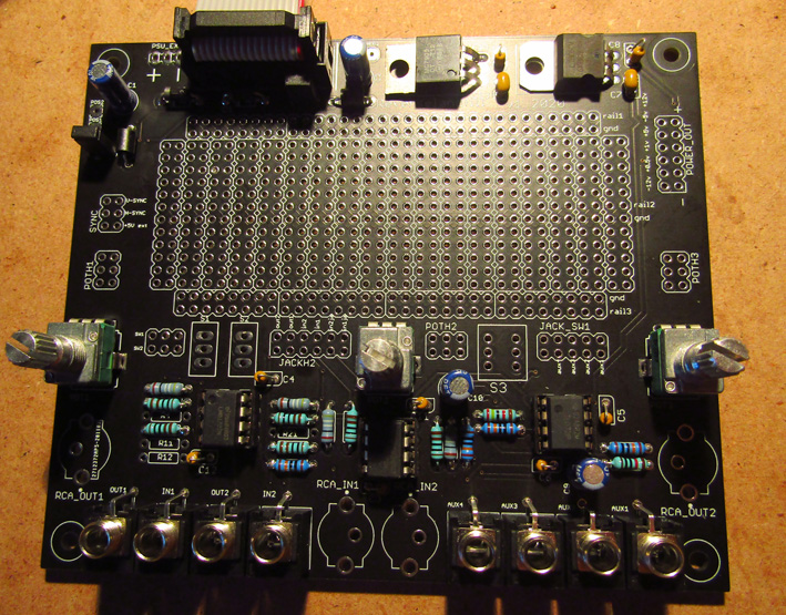
I have 50x pcbs for this run
50x! You’re “all in” Martijn
Thanks for posting the news & photo, it’s really great to see
I’ll attempt another group buy here in Berlin. Just stumbled across another LZX user (Vidiot to be exact) on Fakehook 2 days ago who’s also based here.
I have a few hopefully-helpful silkscreen comments/suggestions, mostly in the spirit of putting as much info on the silkscreen as possible so someone using it never has to guess about a header or refer back to documentation to make sure about something…
It’d be nice if the silkscreen explicitly showed the connections and rails unambiguously for the breadboard area. As it is now, the silkscreen makes me think that every two rows are connected (like a 2x5 or 2x6 header), instead of just single rows connected (like a 1x5 or 1x6 header). Also the middle rails aren’t obvious. And the silkscreen makes me think the side rails might be separated every 8 holes.
Similarly, it’d be nice if the pot headers showed which pins are connected. One can assume that it’s 3 groups of 2 connected pins, but it’d be nice to be explicit.
It’d be nice if the jack headers were labeled a bit more, since from the last pcb layout you posted it looks like the two rows of holes are not simply doubled up as they are for the pot headers. I presume one row is jack and one row is jackswitch, but if that is the case, the silkscreen doesn’t seem to indicate which is which as far as I can tell.
If you rotate the labels for the Power Out holes you can probably fit them next the their respective pins, which I think would be an improvement.
It’d be nice if the PSU EXT headers had the middle pin labeled too. I presume it’s ground?
I know this isn’t the best timing, since you already ordered and received the first batch. Sorry. But maybe consider these suggestions for the next batch? (I assume you’re going to sell a bunch of these – I know I want several, even if you don’t implement these silkscreen suggestions!)
most things I figured out myself too.
Sometimes you get too focused on certain things, then regret it after you have send the files.
I’ll make an overlay as helpfile
next version update.
breadboard area now has clear markings (on the top and bottom side of the pcb)
pot, switch and jack markings are more clear
power out markings are better
ext PSU has gnd label
connected header pads have lines
The schematic above shows them coming out of U3. The resistor values (R15-18) are all listed as 1K, so they may not have been calculated at the time of posting.
U3 should probably be a TL072 if they are used as unity gain buffers without a negative feedback resistor.
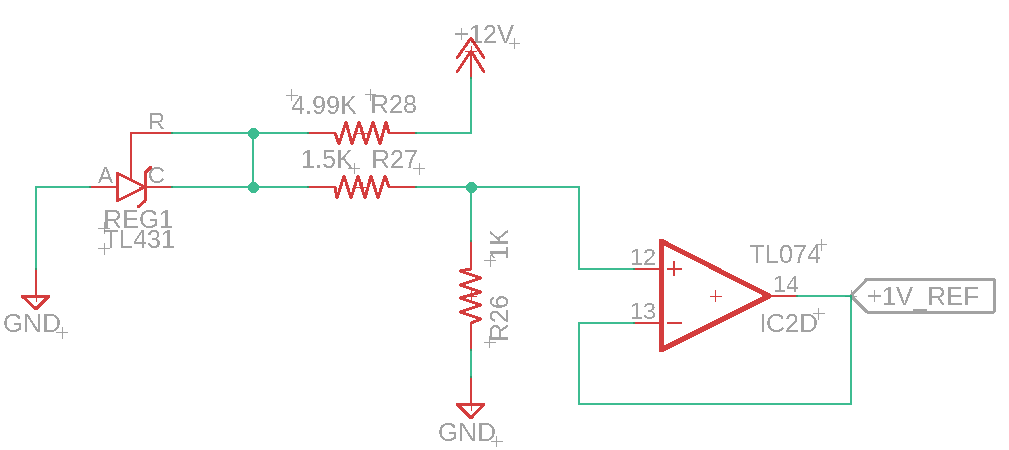
Ah! I see. I was expecting to find a TL431 like the Cadet RGB encoder has, to make sure those voltages are stable even if the power rails aren’t so good. Here’s a circuit I use for reference voltages:
The ratio of R26 : (R26+R27) sets the voltage divide from the TL431’s +2.5V output. To get +0.5V I would use a second voltage divider (1K / 1K) from the +1V_REF into a second op-amp.