Click for Build Guide
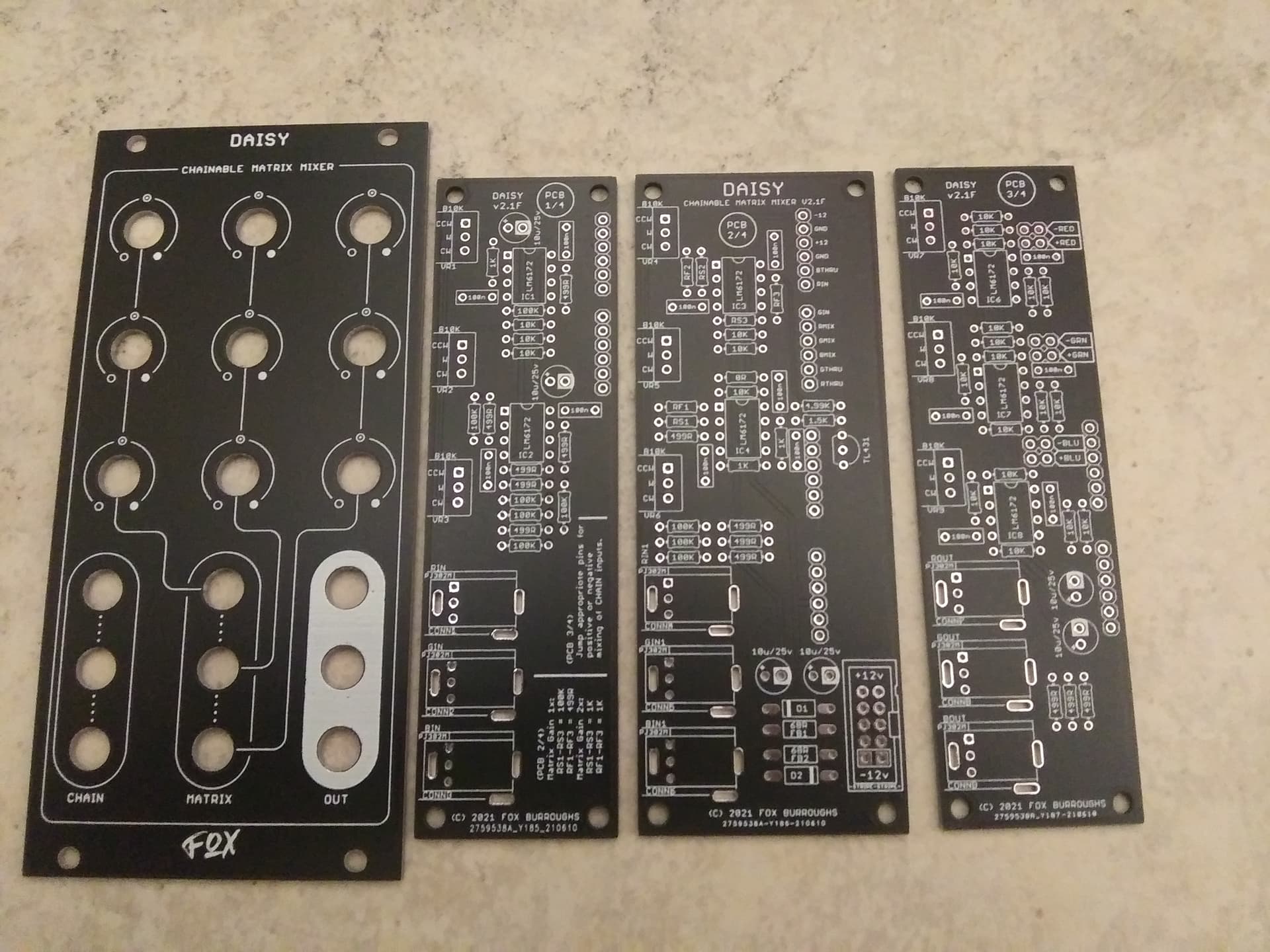
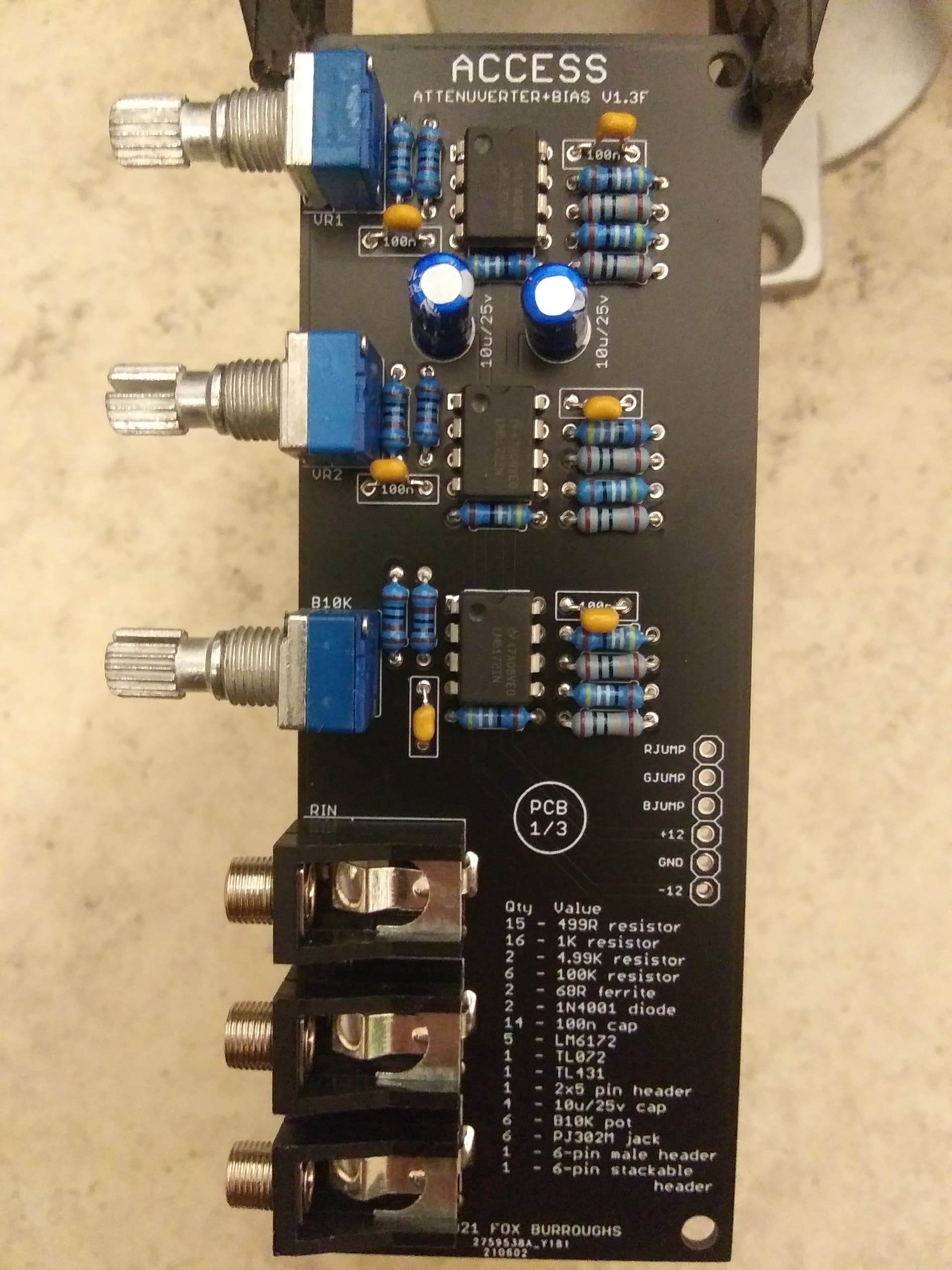
Part 1: DAISY (PCB 1/4)
Step 0.
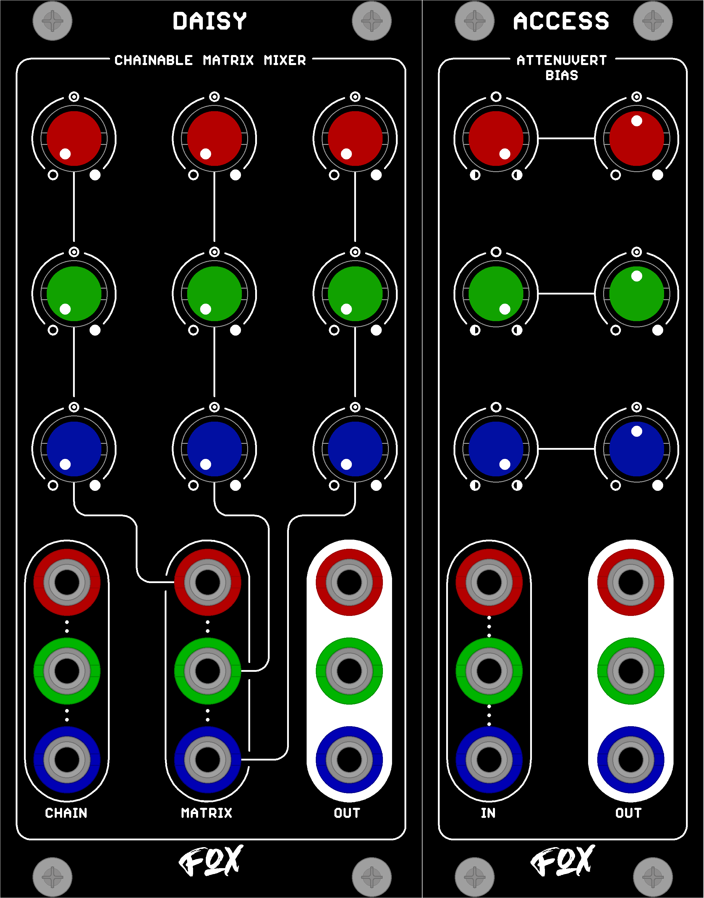
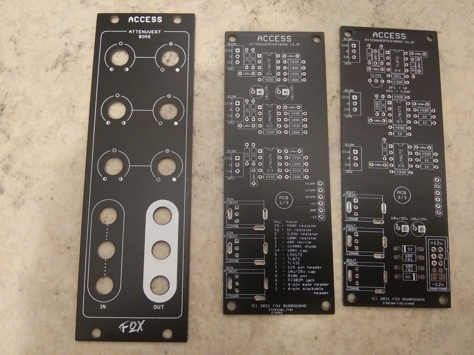
This is the build guide for DAISY v2.1F.
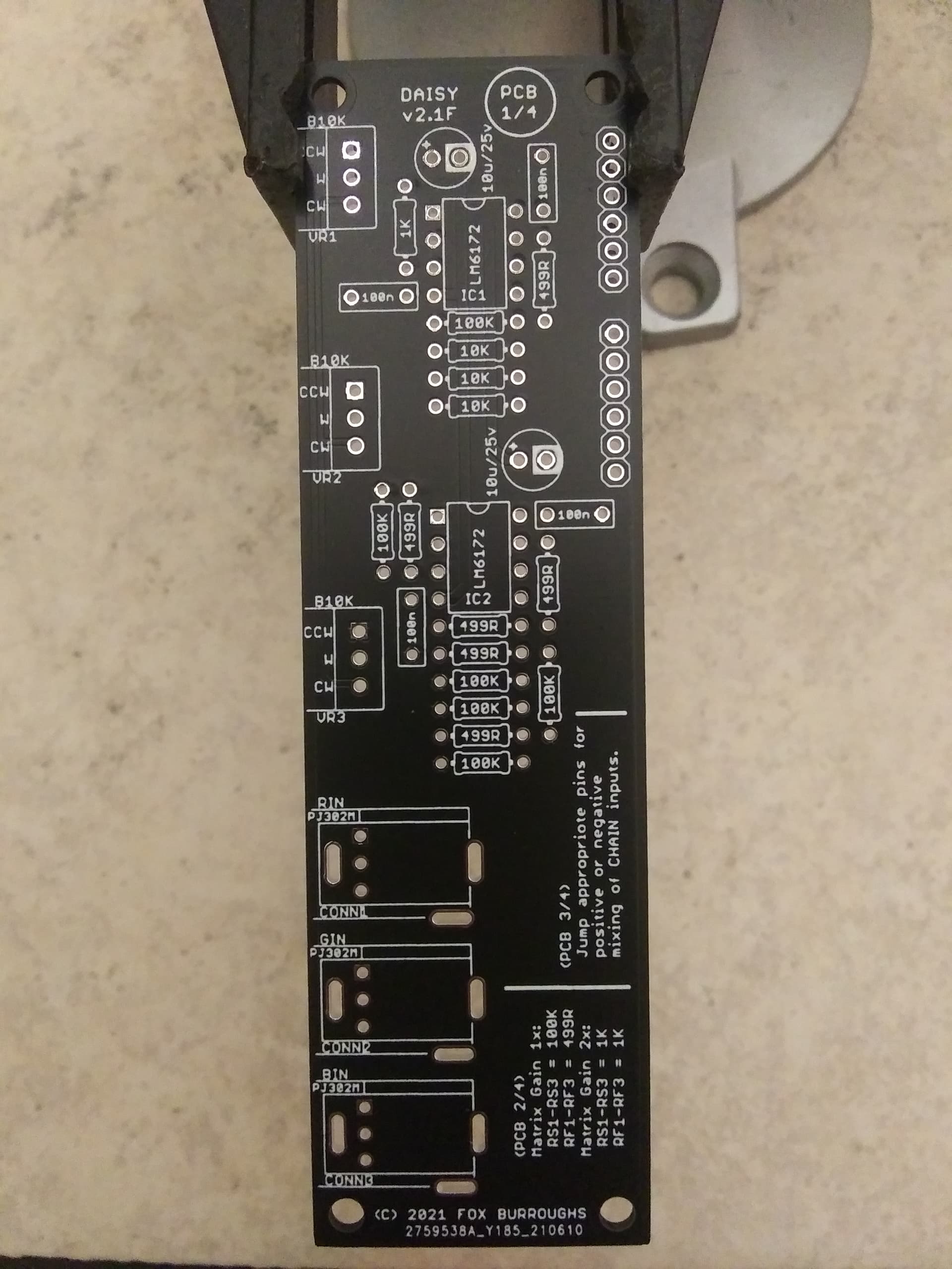
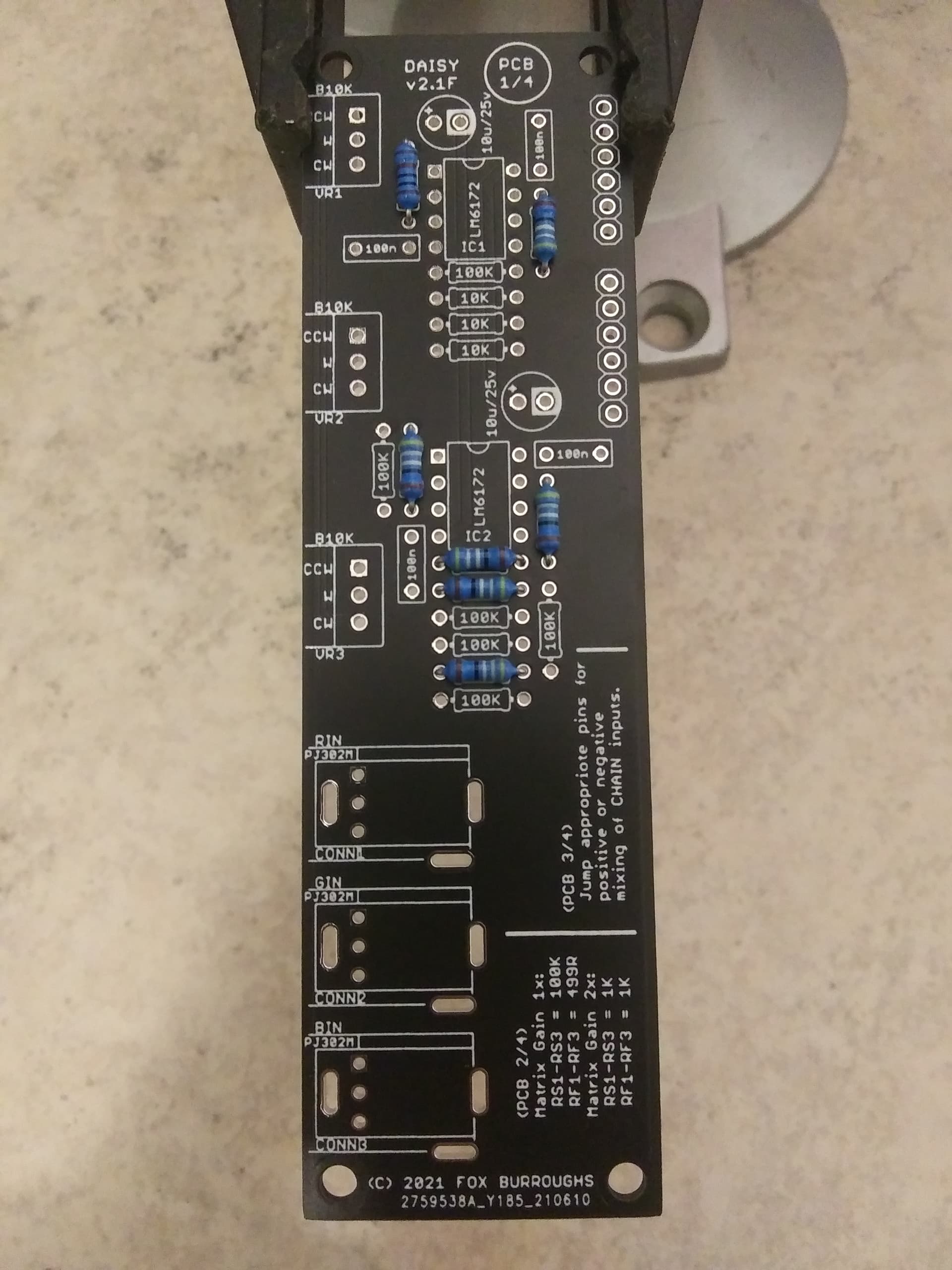
We will start with (PCB 1/4)
Step 1.
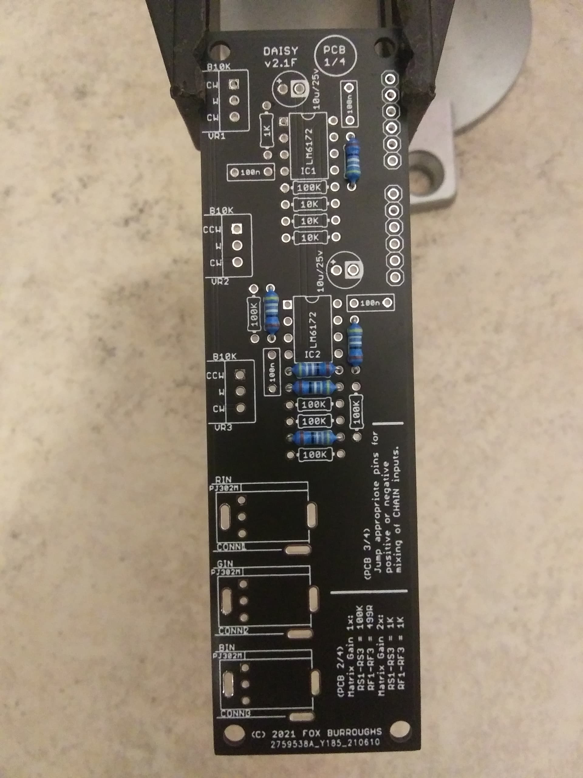
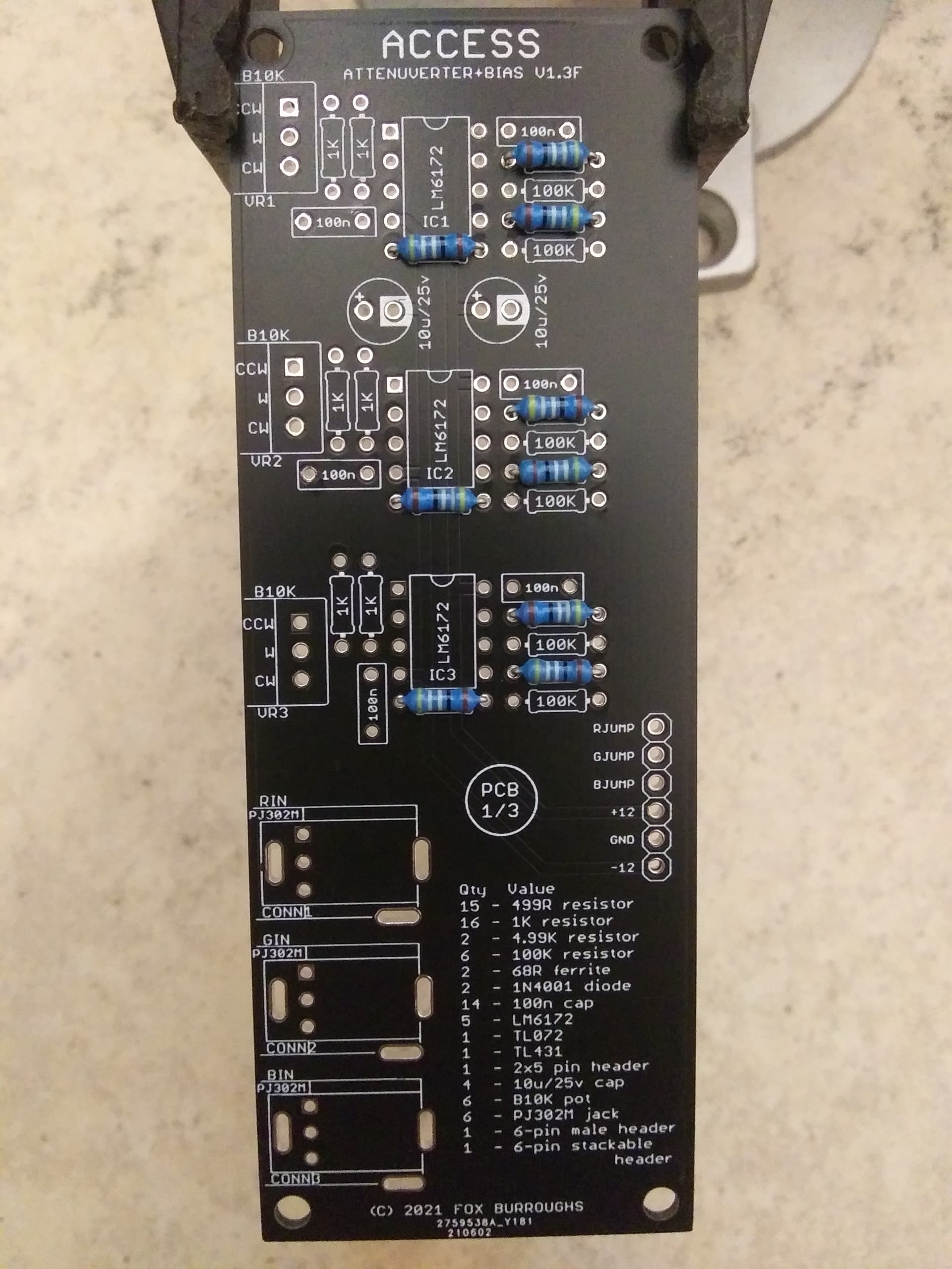
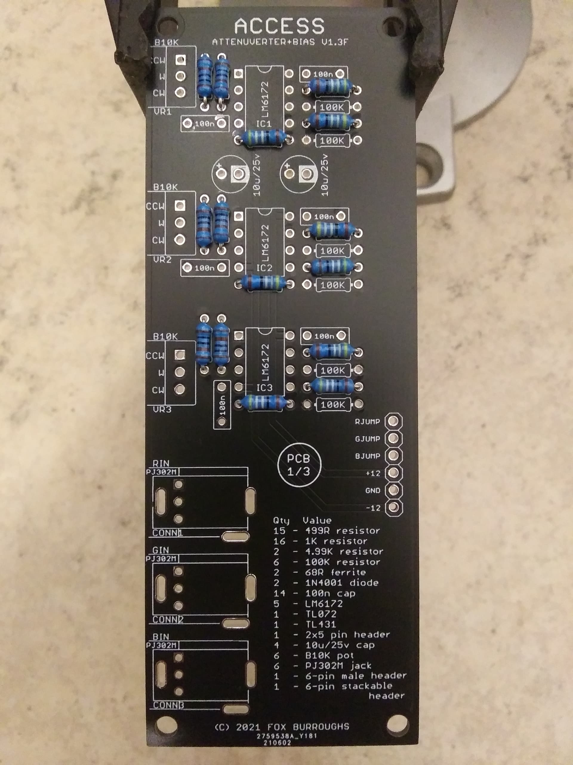
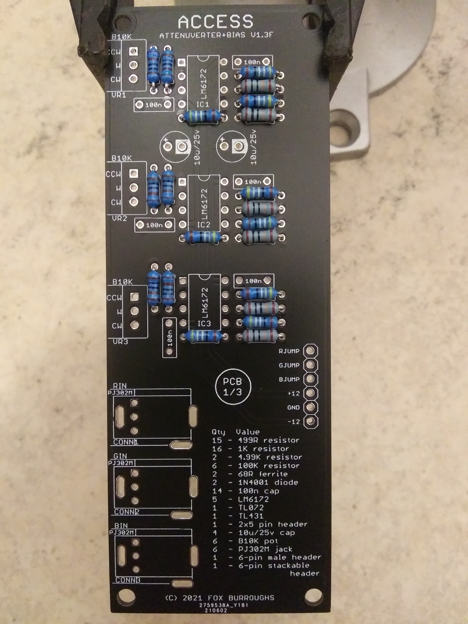
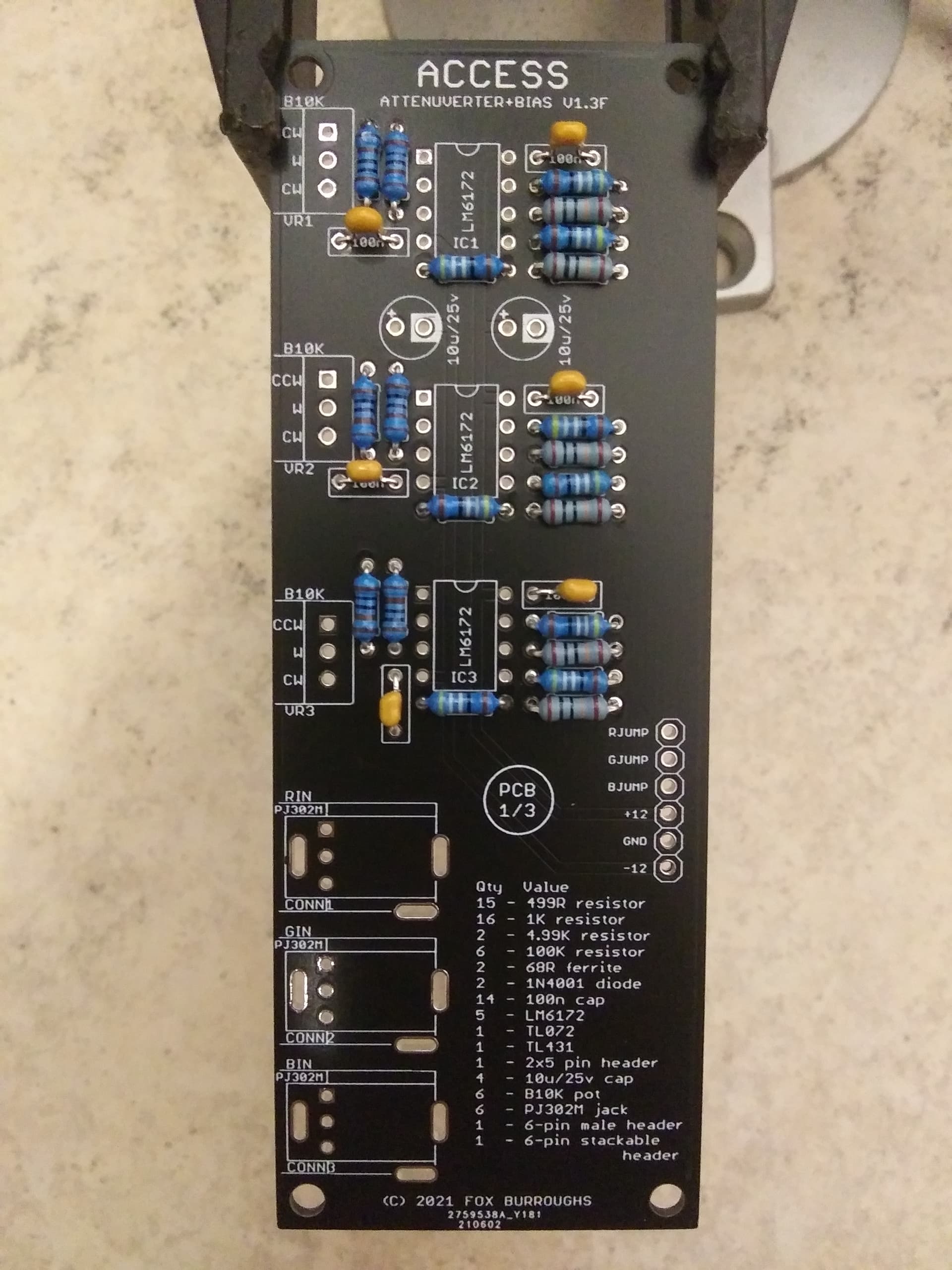
Begin by populating the 499ohm resistors. All 6 are labelled “499R” and pictured below.
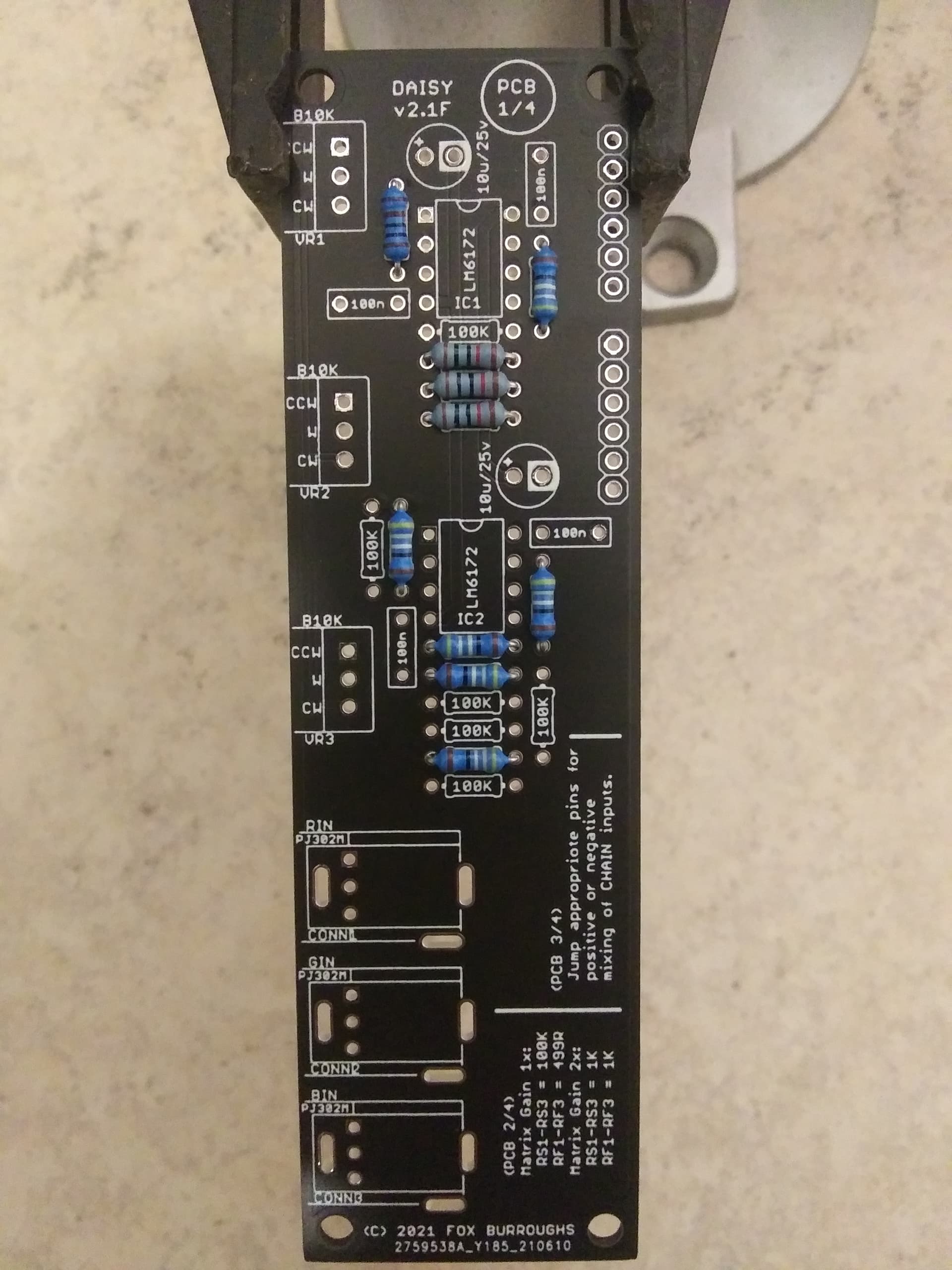
Step 2.
This board has only a single 1Kohm resistor.
Step 3.
Next, populate all three resistors labelled 10K.
Step 4.
The last resistors on this PCB are 100Kohm. There are six to populate.
At this point, I will solder all of the resistors I have populated but you may do so one-by-one if you like.
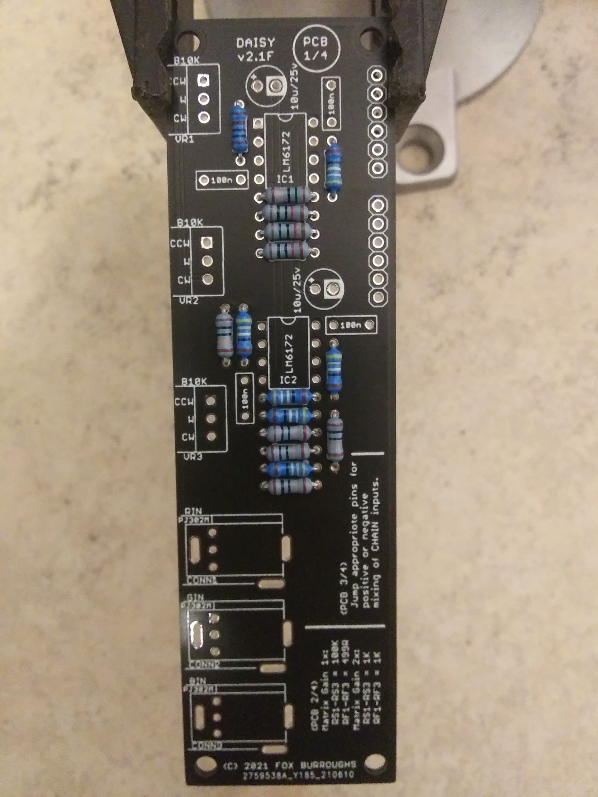
Step 5.
Now that the resistors are finished, we may move on to the capacitors. Here you can see that I am using dipped MLCC-type with a lead spacing of 5.08mm.
There are four 100nF (0.1uF) caps.
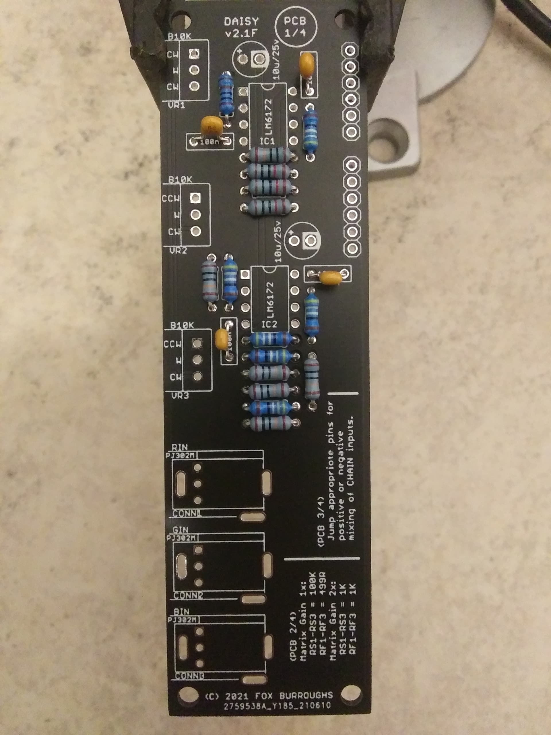
Step 6.
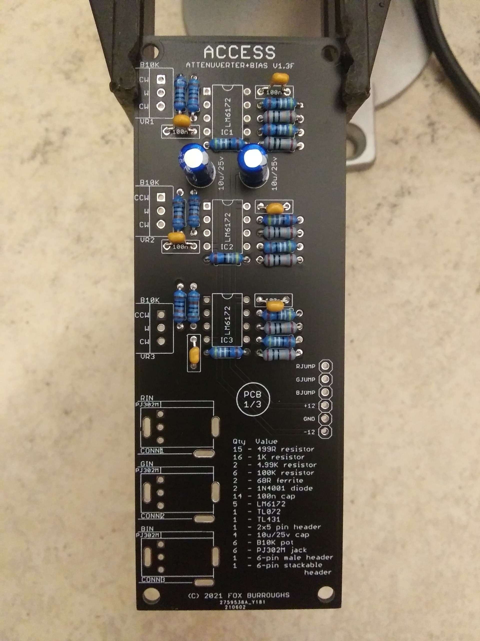
Now we will add both 10uF electrolytic capacitors. These should be rated for at least 25V, but 35V and 50V may still have a lead spacing of 2.54mm. Pictured below are 50V rated caps.
We are using polarized electrolytic caps here, so be sure to line up the negative lead with the hole outlined in white and the positive lead marked with a “+”.
Step 7.
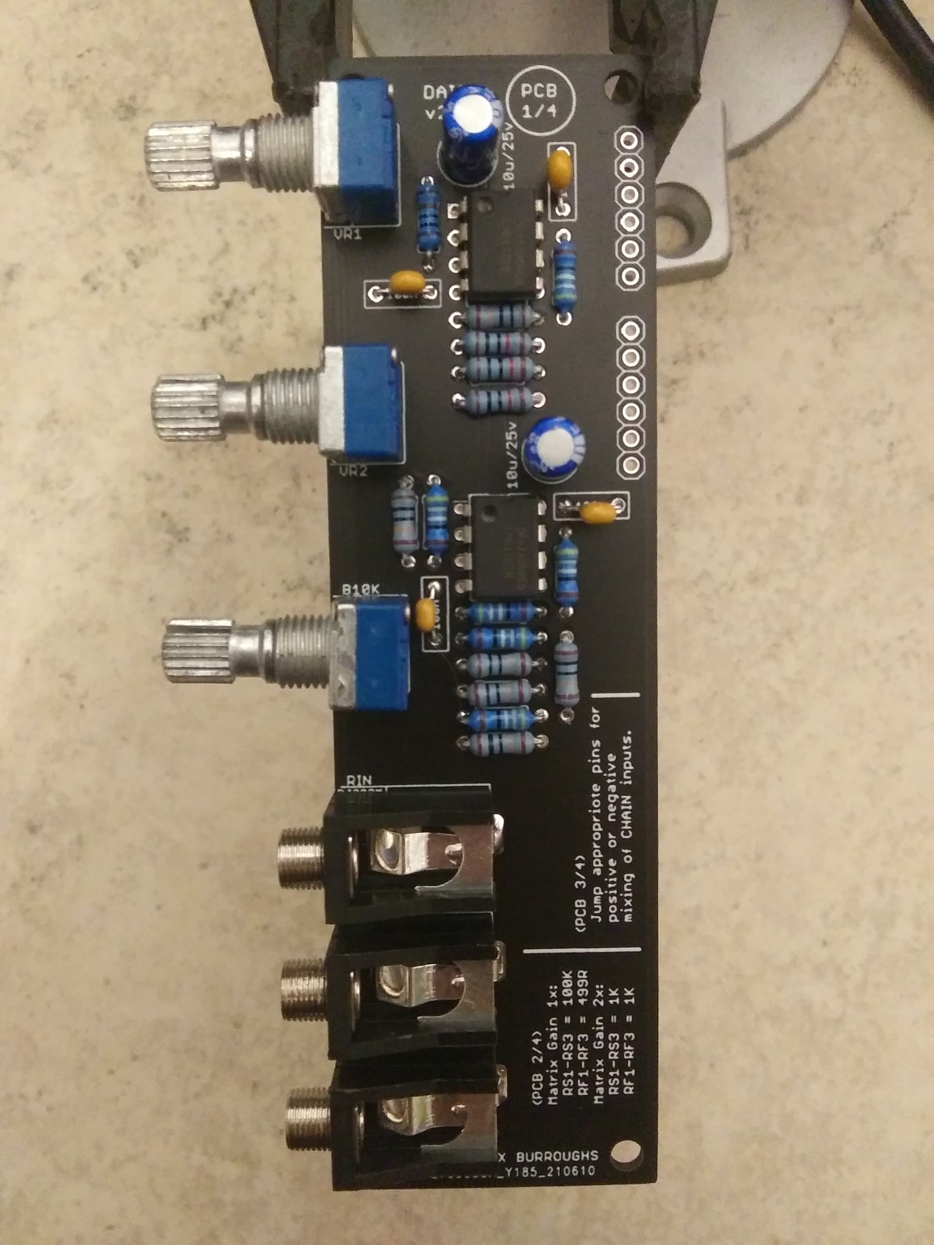
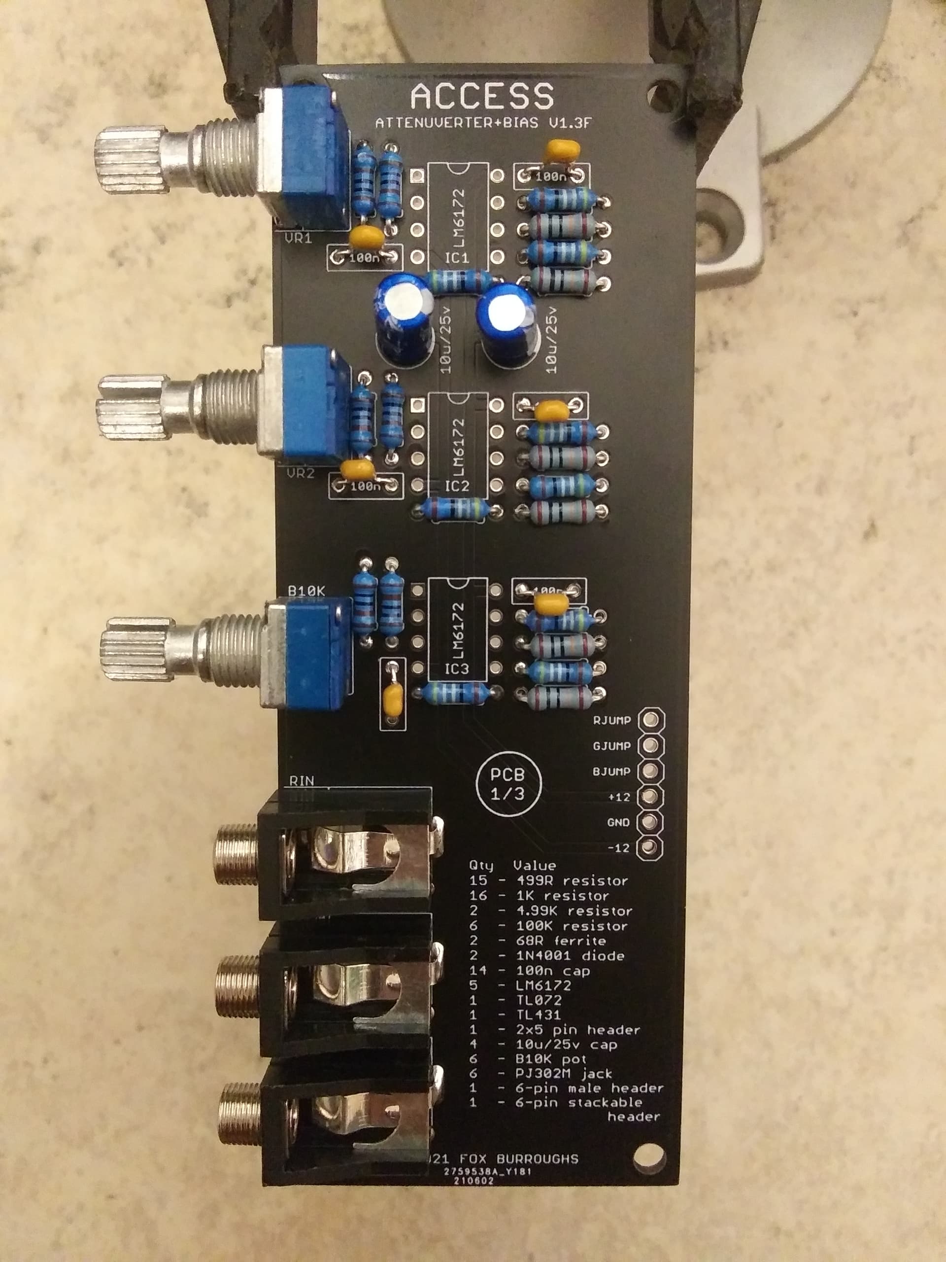
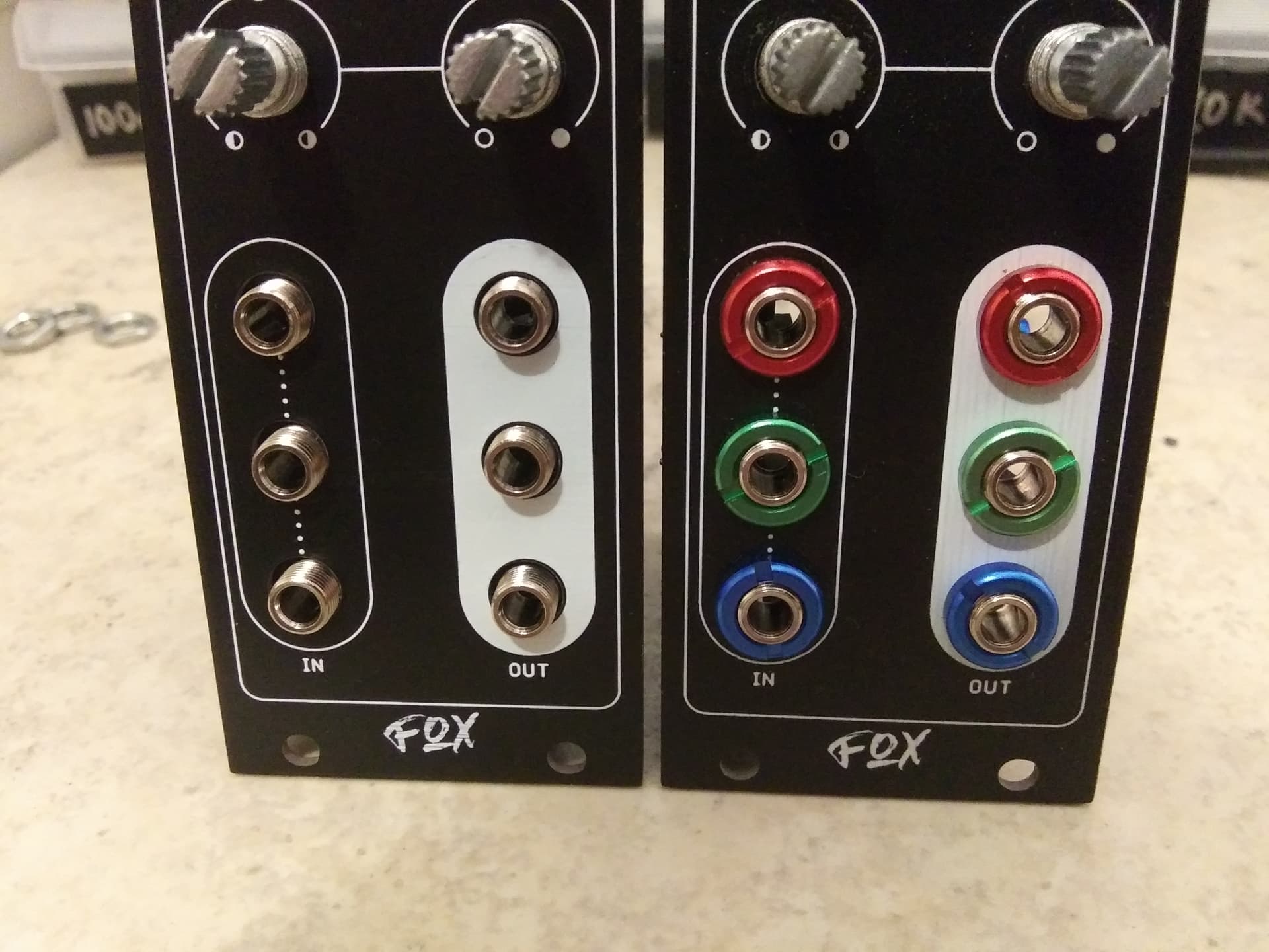
Now we may add the pots and jacks. There are three of each. As a reminder, we will need to use Linear taper, 10Kohm, right angle pots with a T18 shaft.
Place each component into it’s appropriate footprint and then install the loose board into your faceplate. Hand tighten a nut onto each part and make sure they are lined up straight before soldering.
Remove the faceplate.
Step 8.
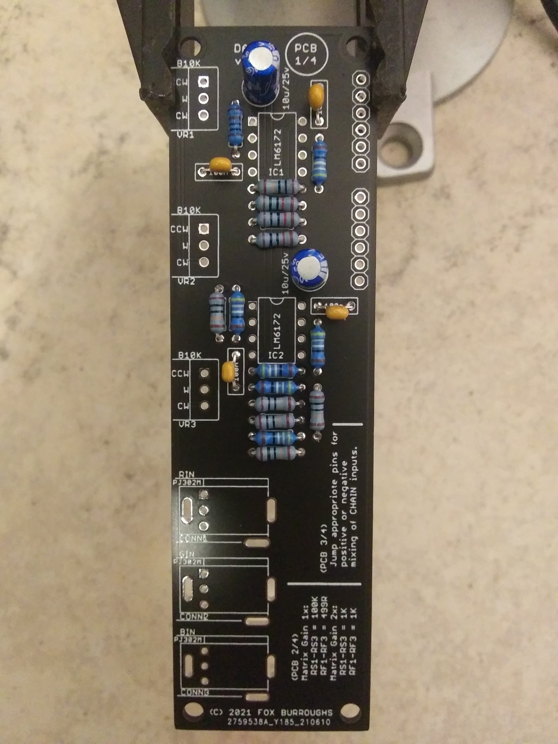
I like to save the op amps for last. There are two LM6172’s on this PCB. Make sure the dot designating pin 1 faces to the top right of the PCB. Pin 1 on the board is also seen using a square-shaped via.
We can now move on to (PCB 2/4)
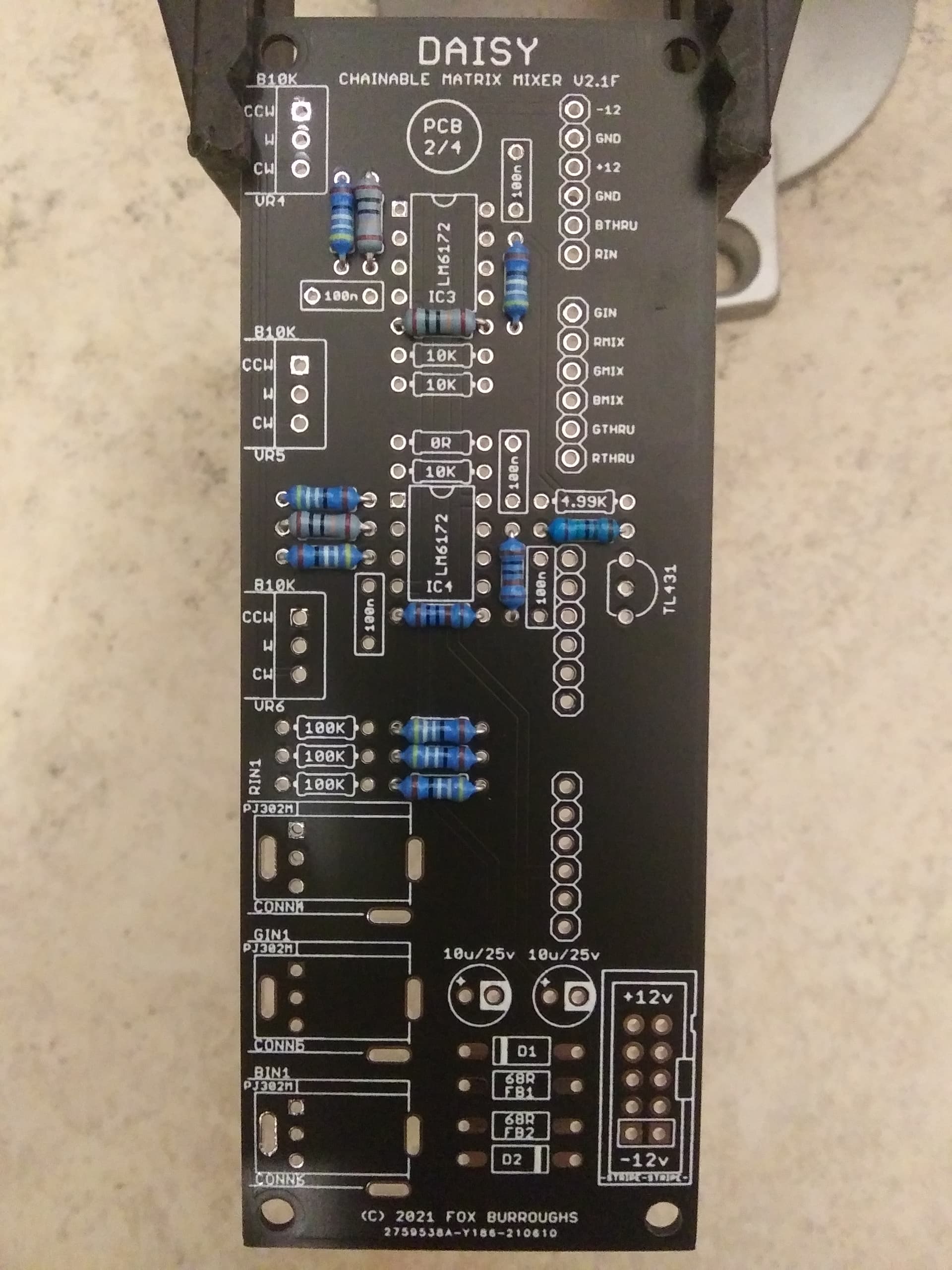
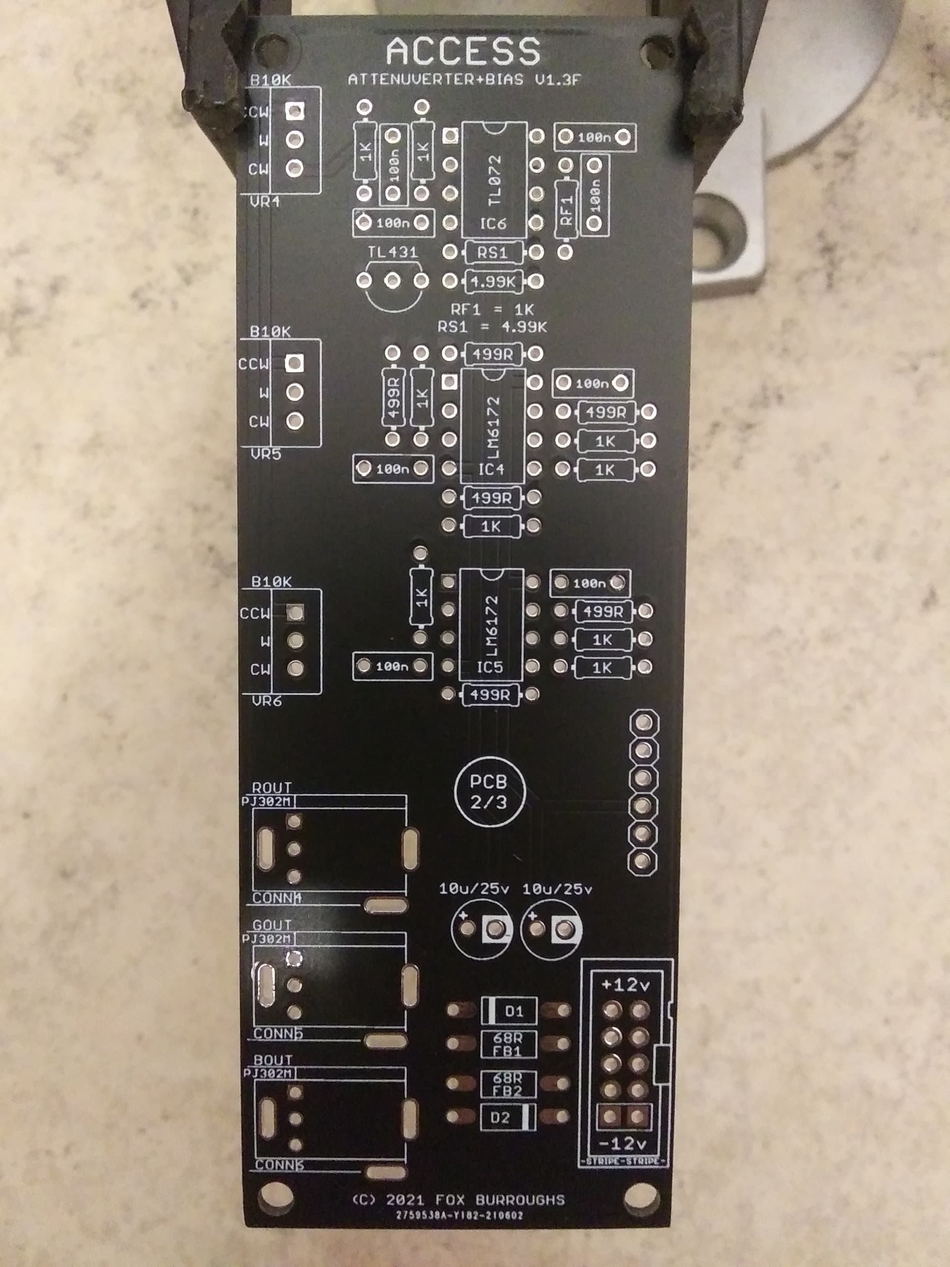
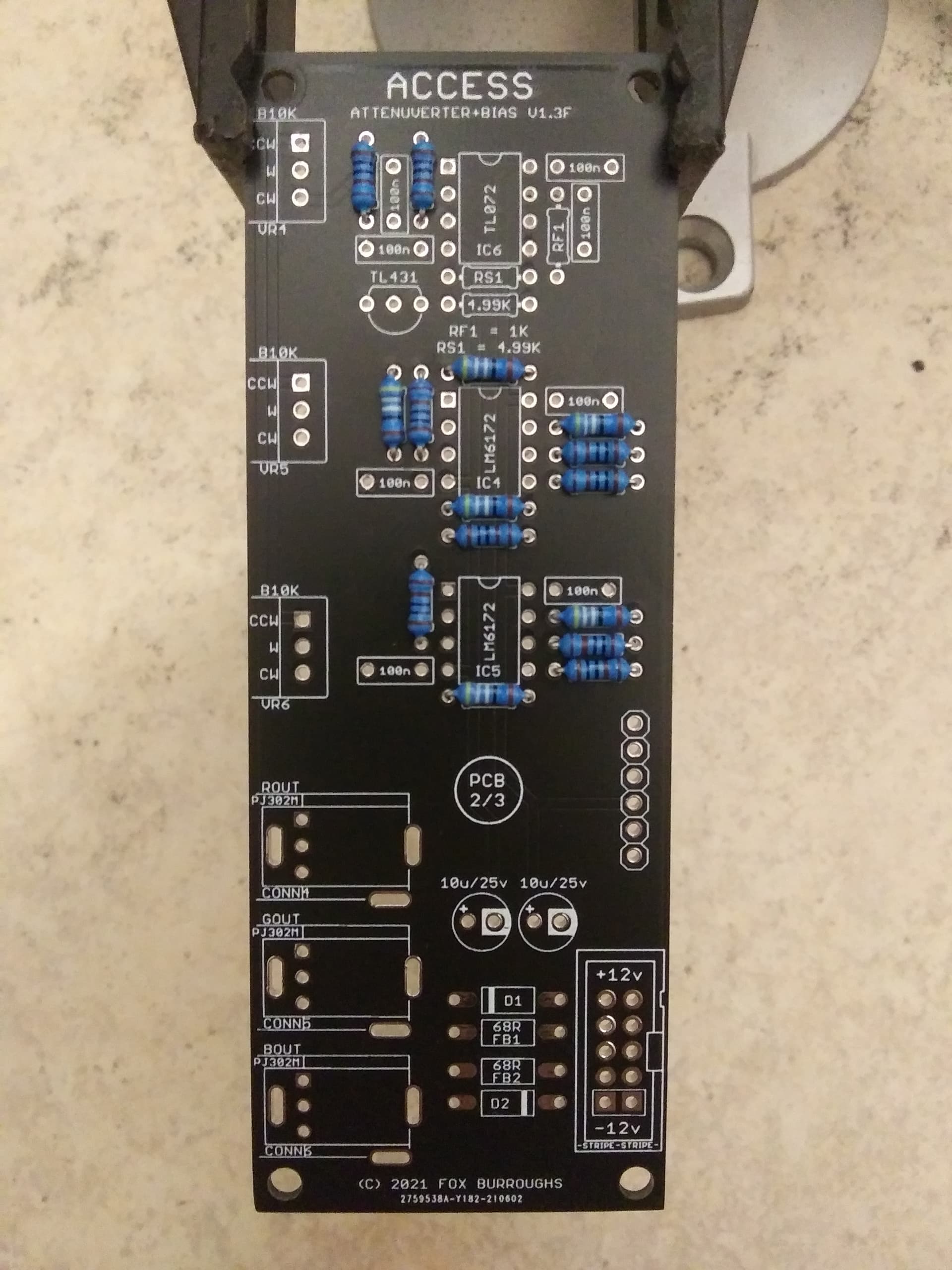
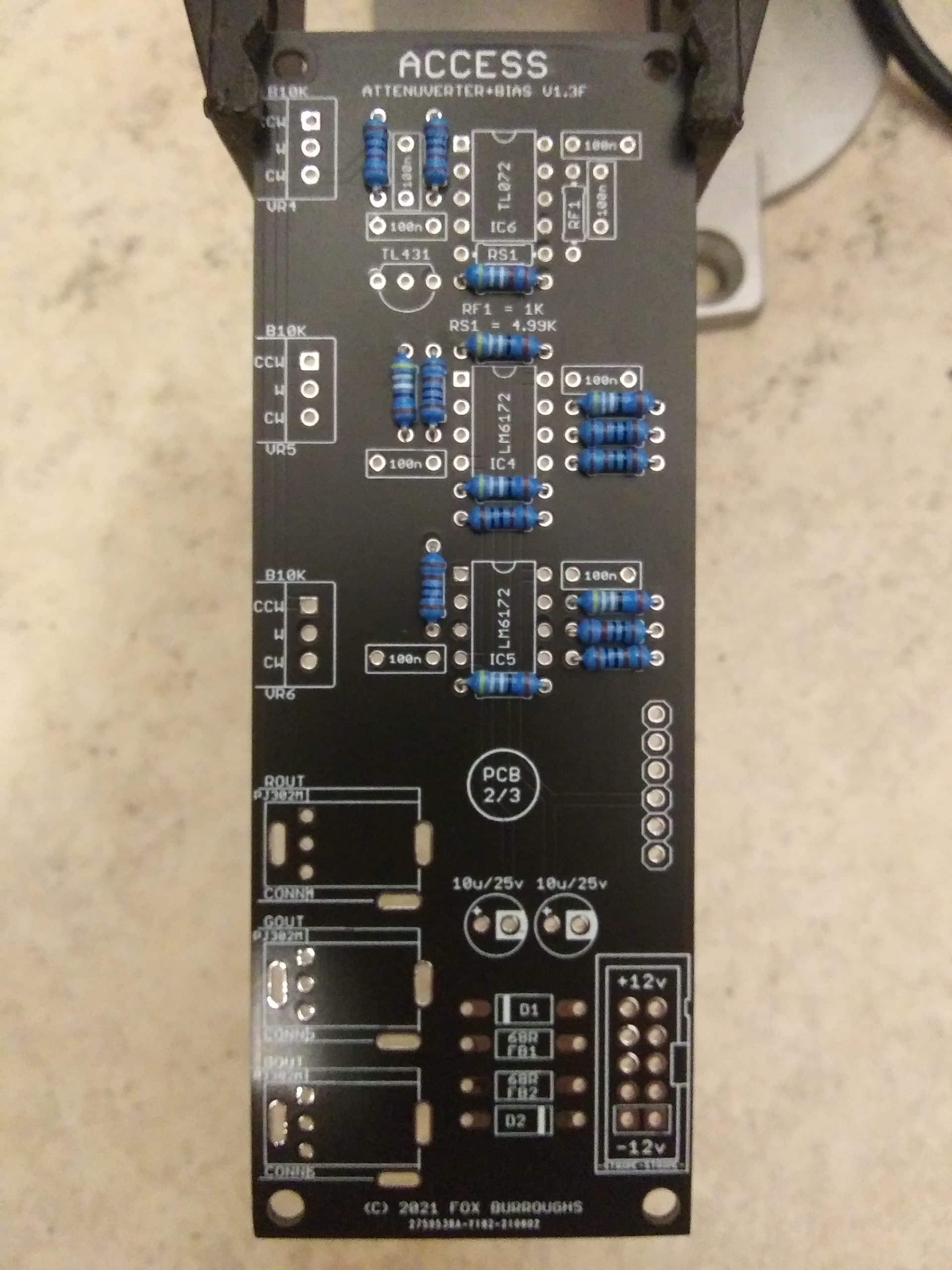
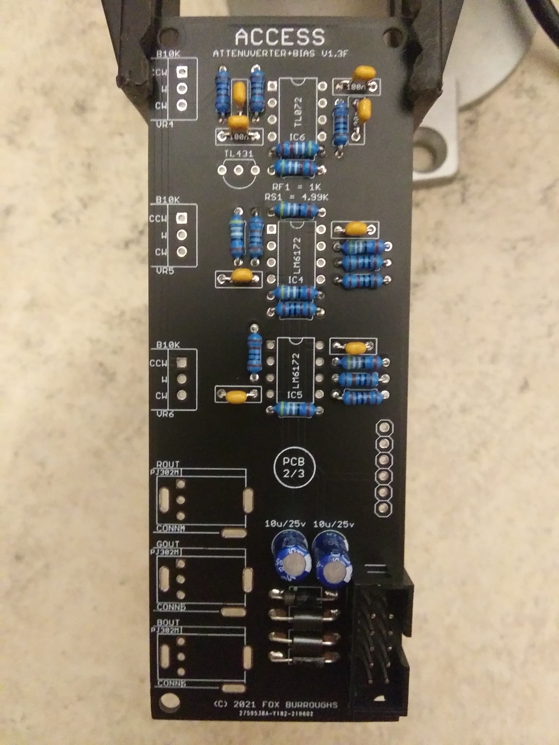
Part 2: DAISY (PCB 2/4)
Step 0.
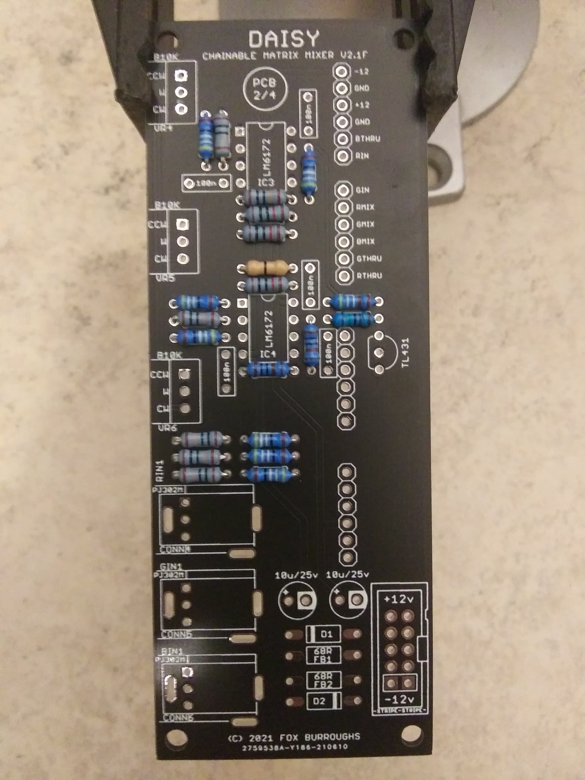
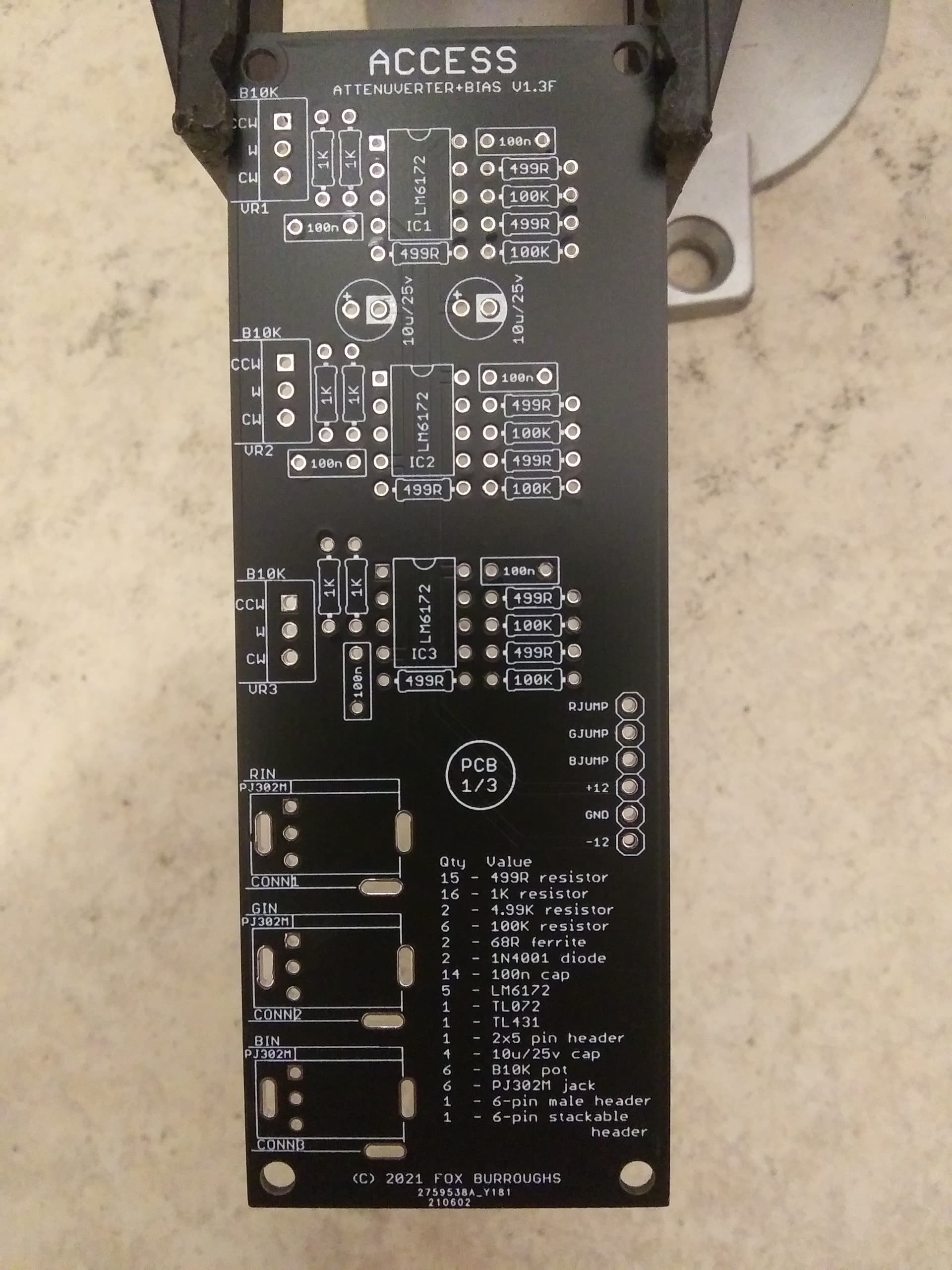
Begin by locating (PCB 2/4) and place it in your vise.
Step 1.
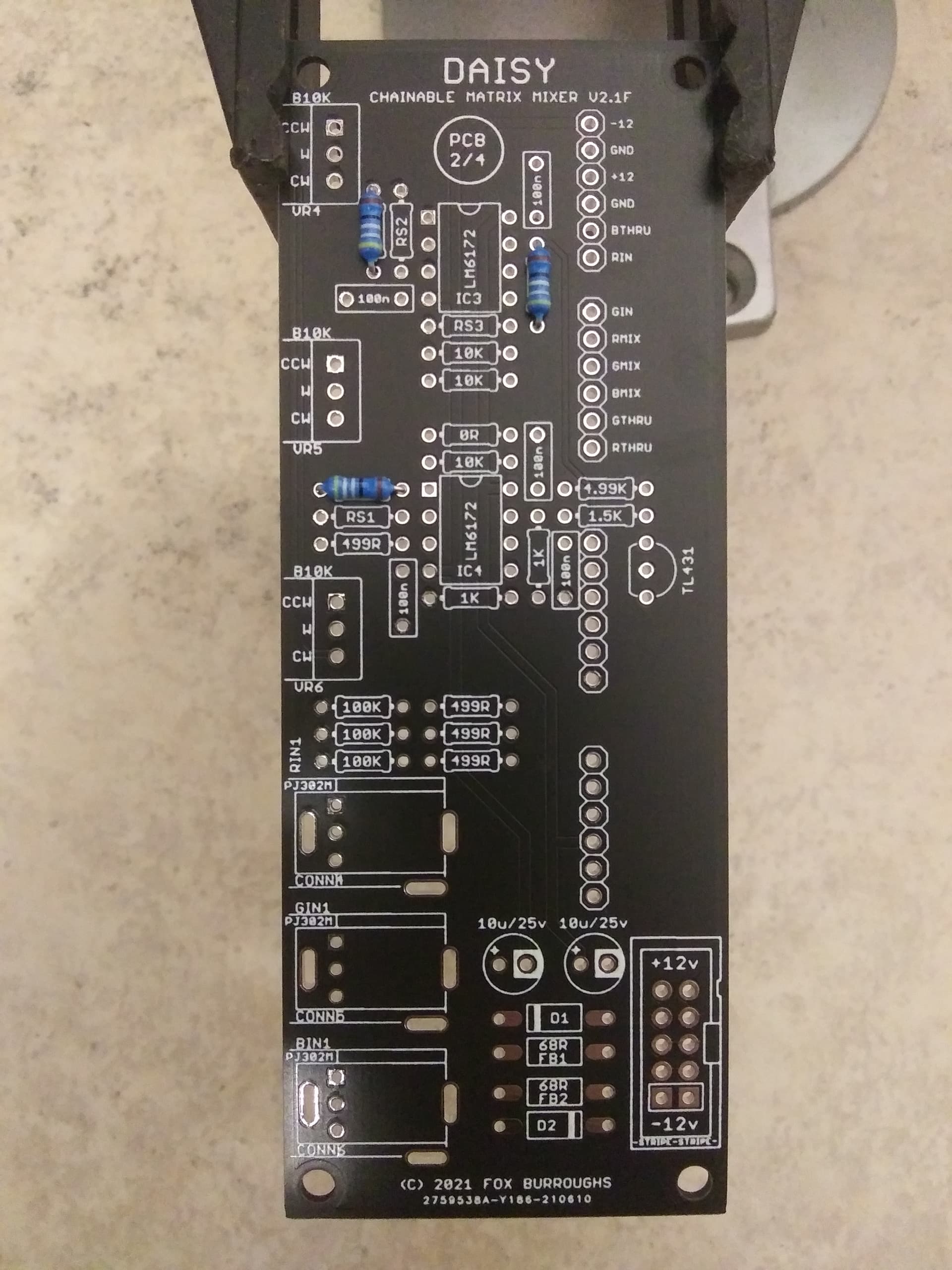
This step populates six special resistors labelled RF1-RF3 and RS1-RS3.
As you may have read on (PCB 1/4), These resistors set the input gain for the “MATRIX” inputs to either 1x or 2x. I recommend 1x gain which means we will populate RF1-RF3 with 499R resistors and RS1-RS3 with 100Kohm resistors.
For 2x gain, all six will be 1Kohm resistors.
Pictured below I have populated the board for 1x gain as recommended.
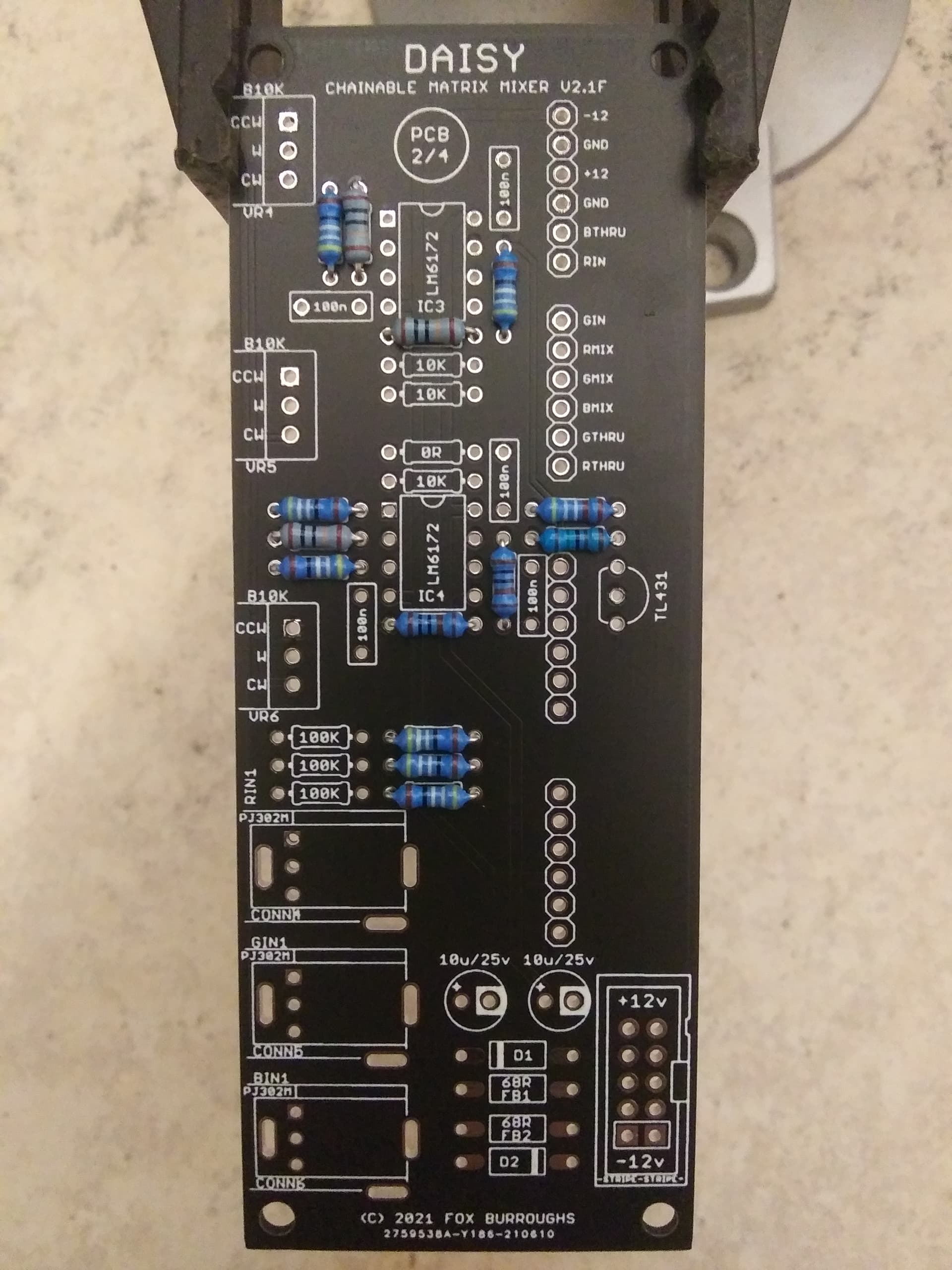
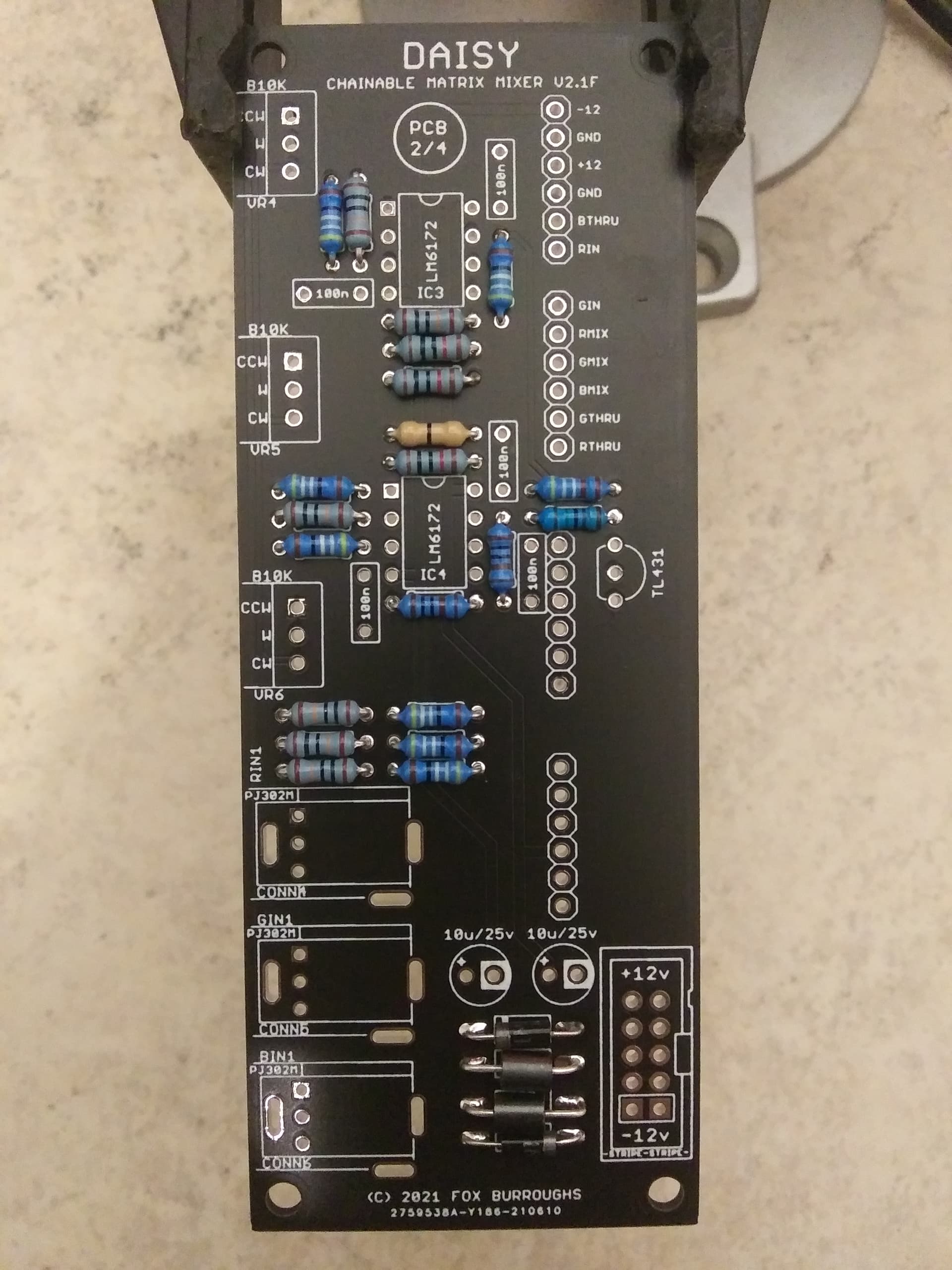
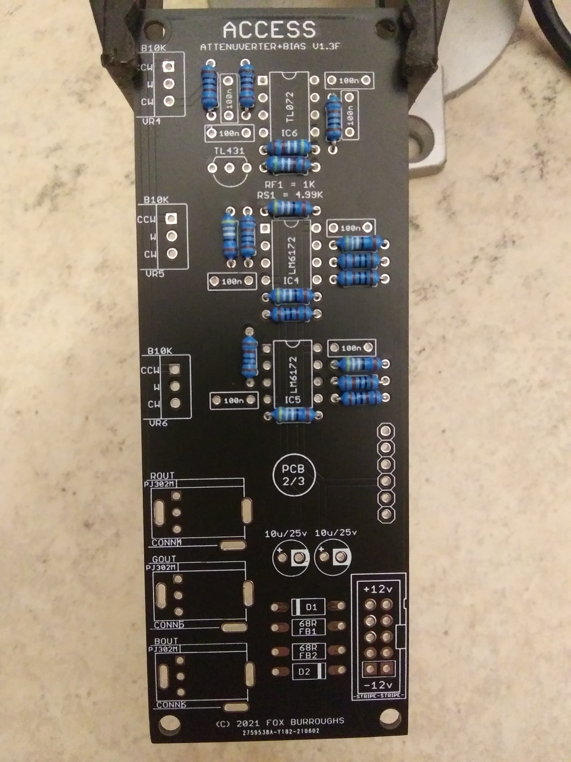
Step 2.
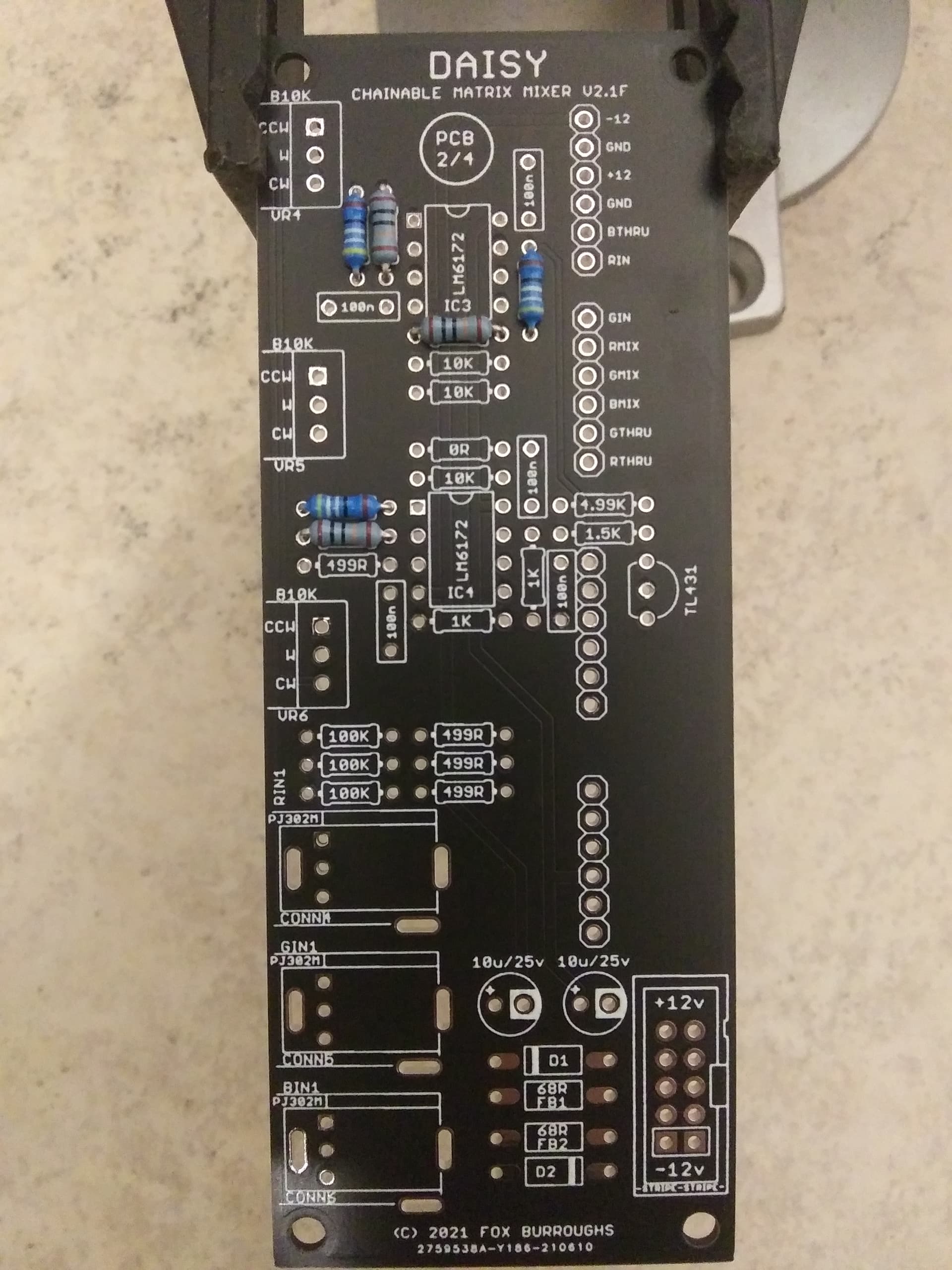
Now we can populated the remaining 499ohm resistors. There are four more, all labelled 499R.
Step 3.
Next we will populate both 1K resistors located under and beside IC4.
Step 4.
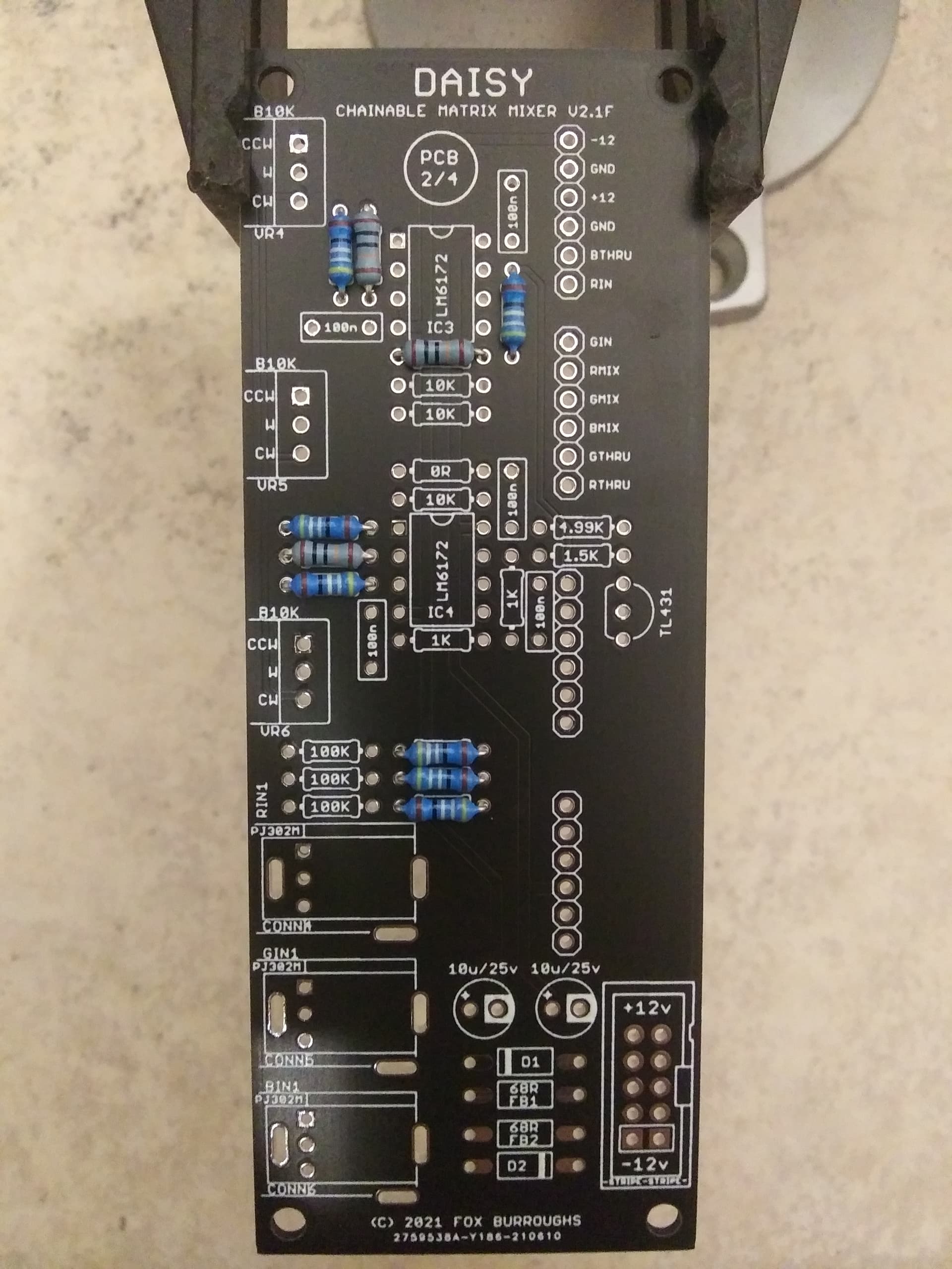
The next resistors set our 1V reference which is normalled to the Red matrix input.
First a 1.5K resistor and then a single 4.99K resistor.
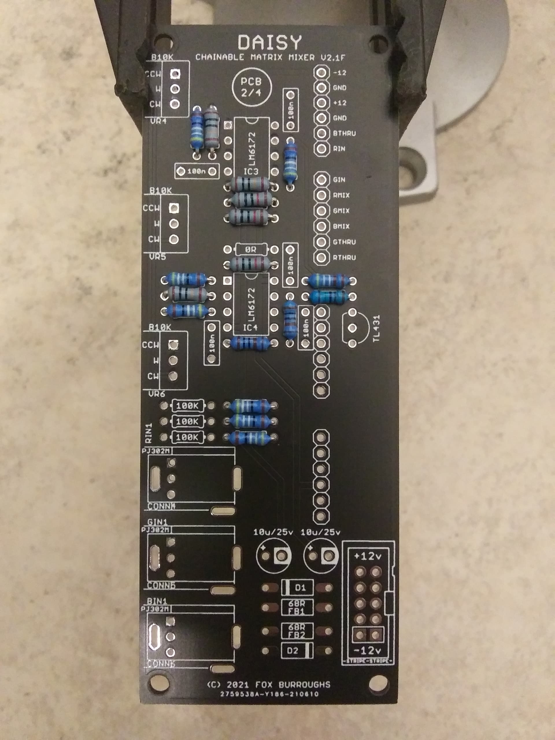
Step 5.
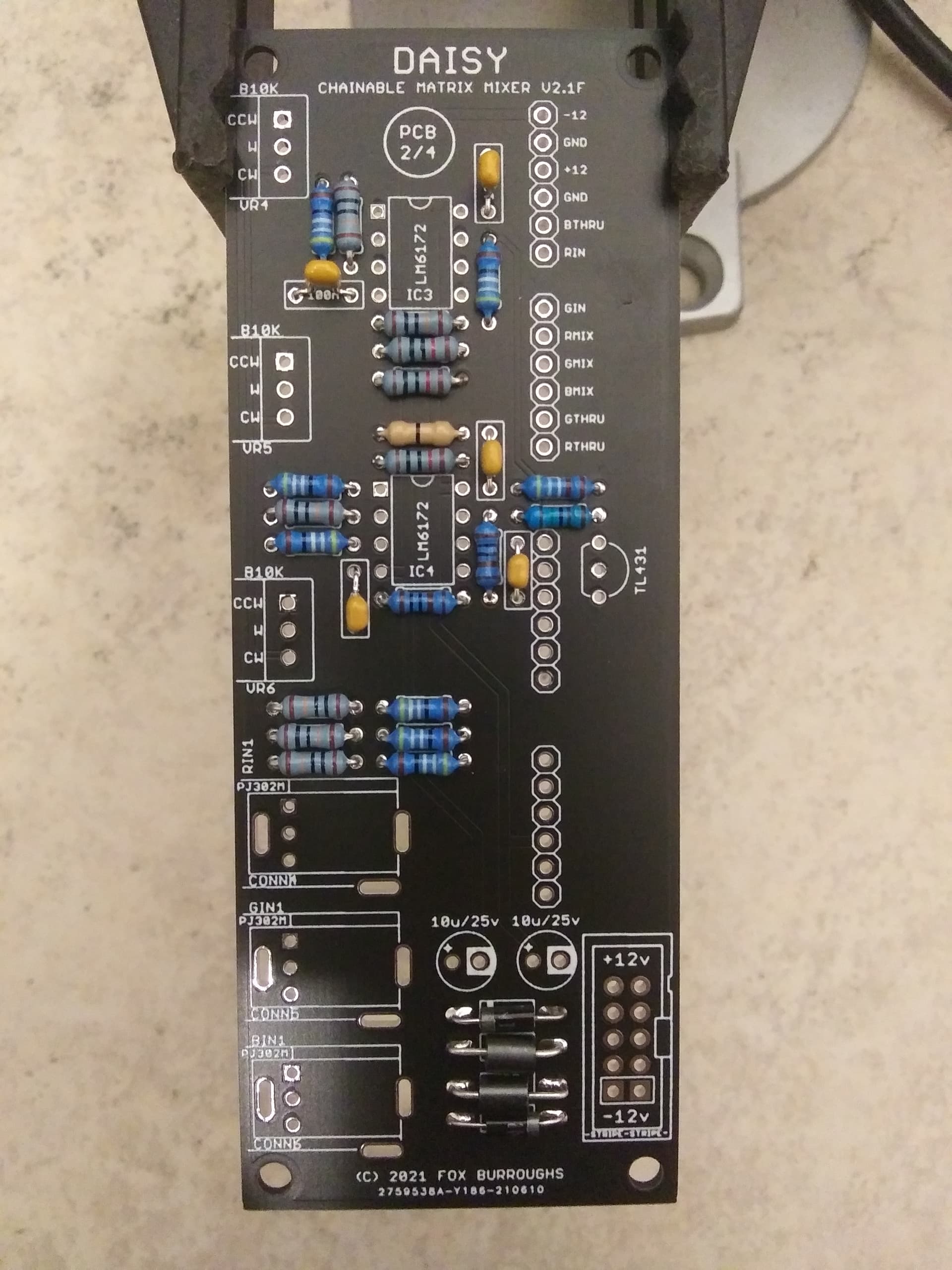
In this step, we populate three 10K resistors.
Step 6.
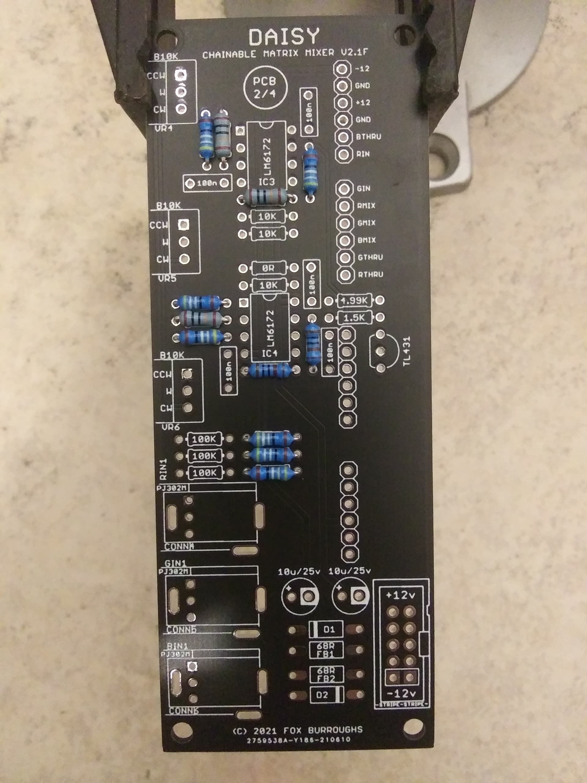
Nest we will populate the remaining three 100K resistors.
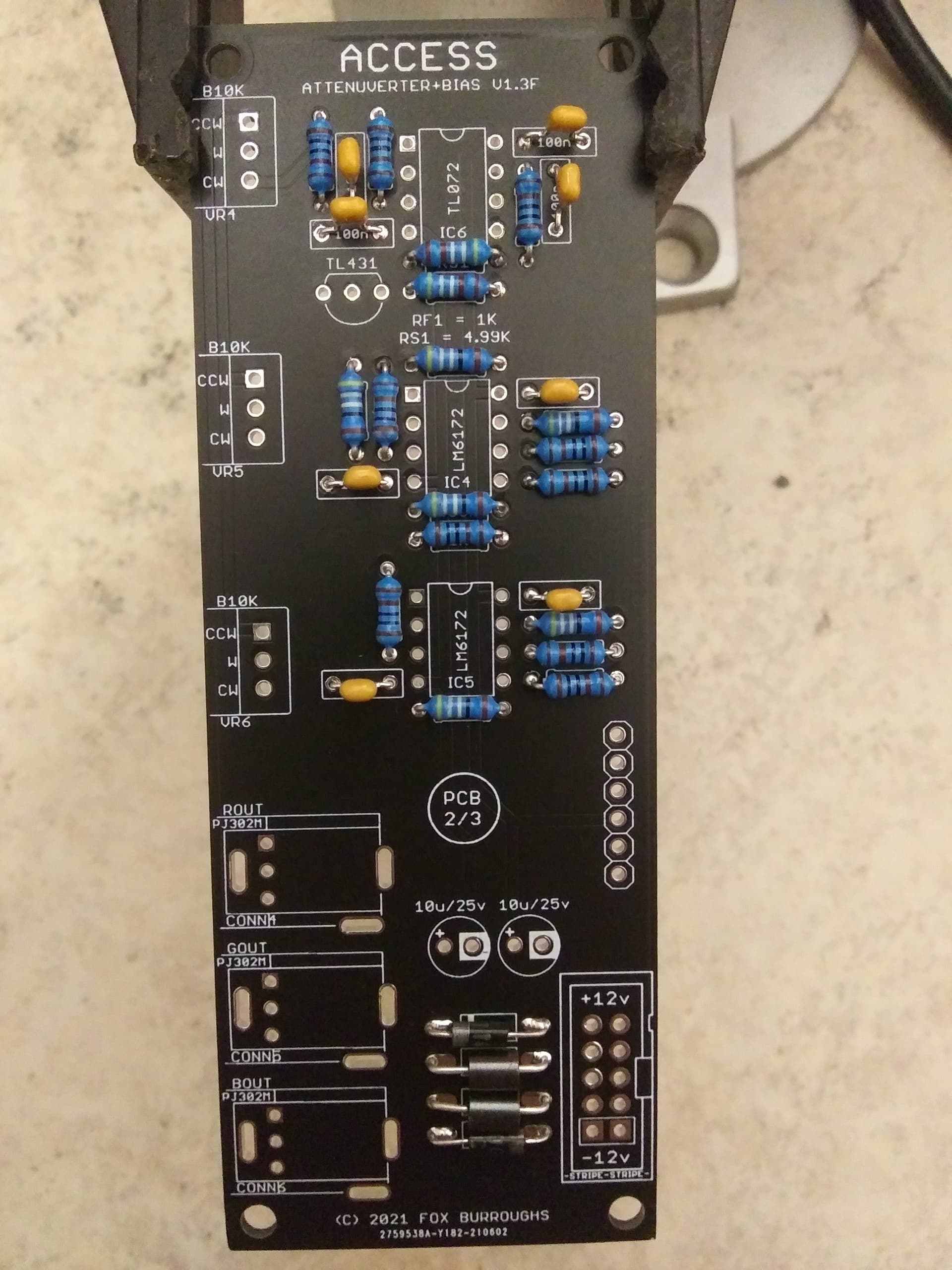
Step 7.
This step adds a 0 Ohm resistor labelled “0R.” If you do not have any 0 Ohm resistors, you may use a clipped-off leg from one of your other resistors. It acts merely as a jumper.
At this point, I soldered all of the resistors in place, but you may have done so while placing them.
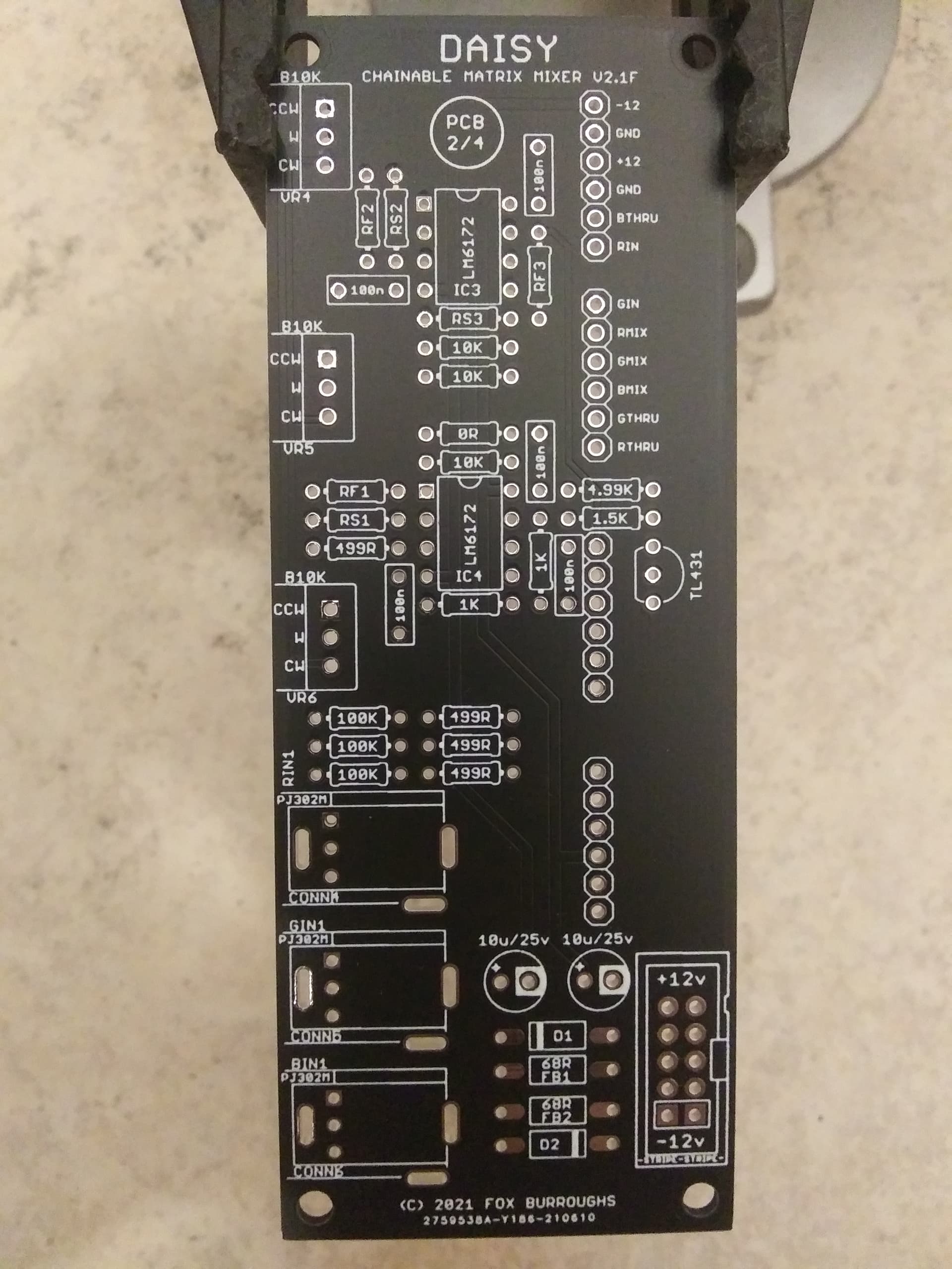
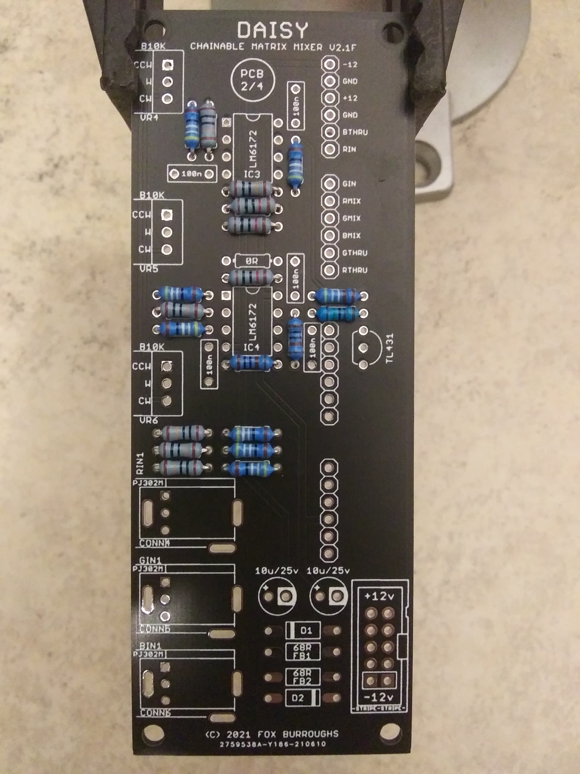
Step 8.
For this step we can add two diodes and two ferrite beads. Diodes are polarized, so DIYers must line up the white stripe on each diode to the white stripe on the PCB.
Step 9.
Now that all of the flat passives are finished, we can place the decoupling caps. There are five 100nF (0.1uF) caps on this PCB.
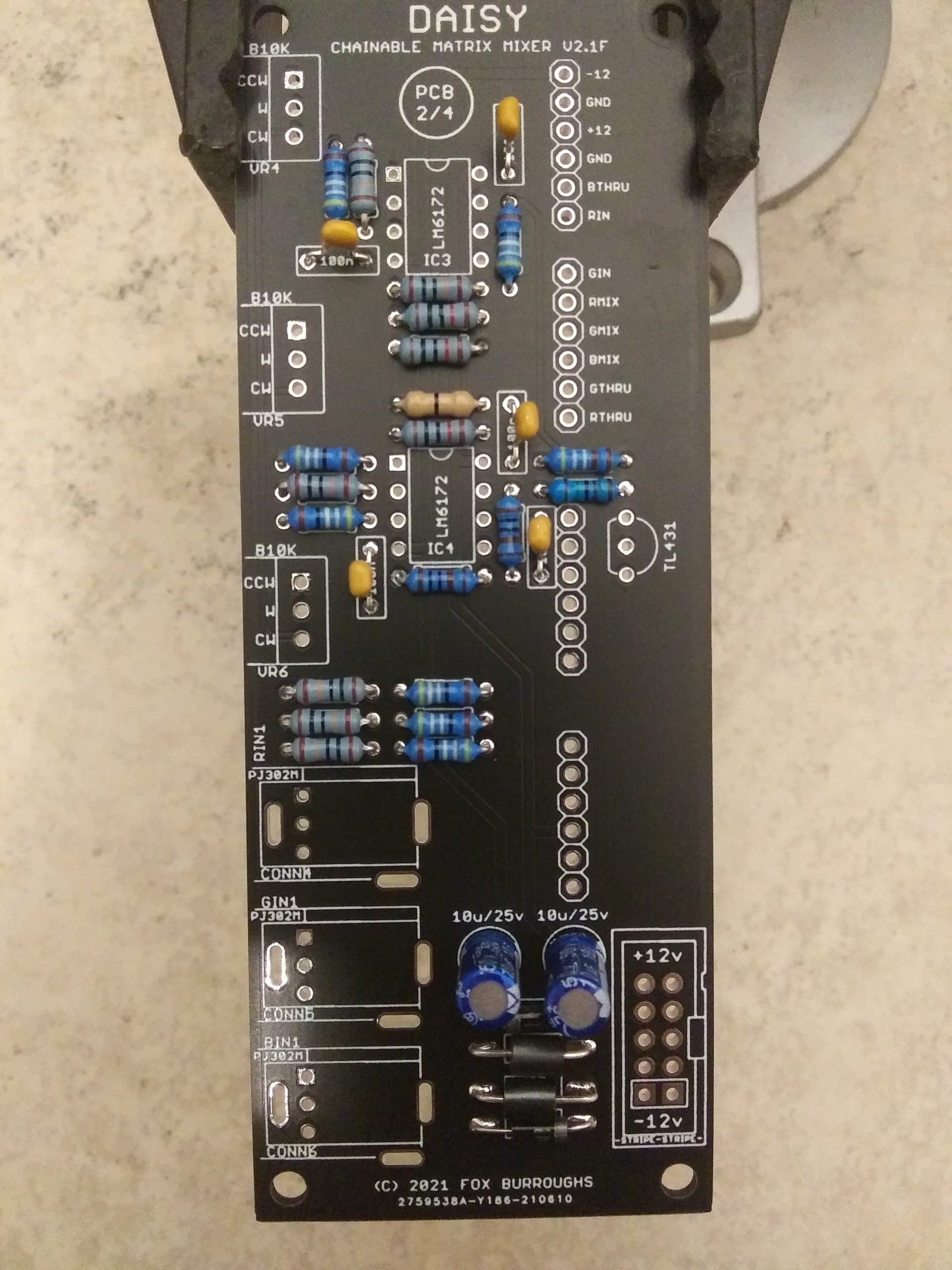
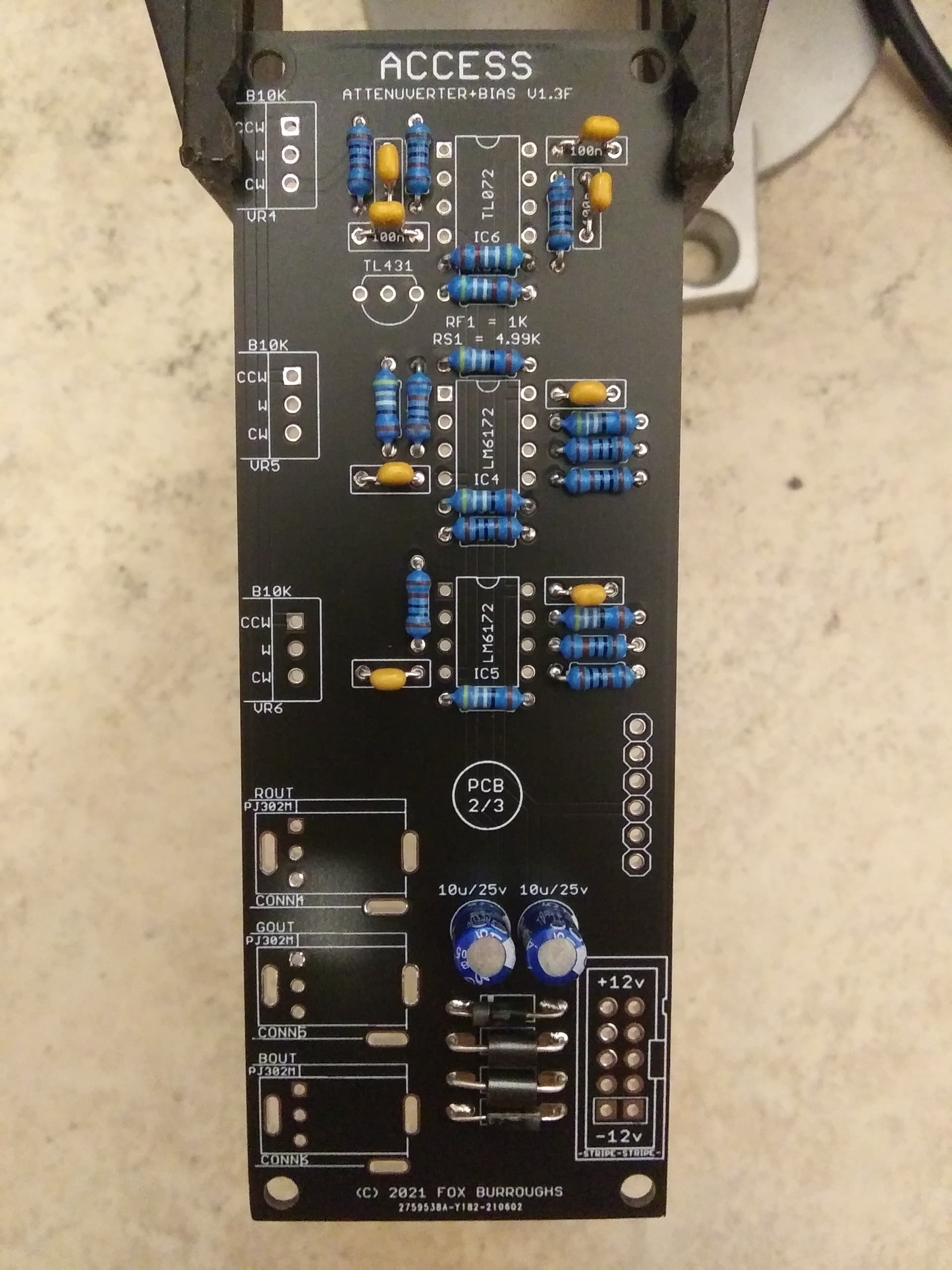
Step 10.
Now populate two more 10uF electrolytic caps. Again, these are polarized and need to be placed correctly. The stripe on your cap identifies the negative lead which will be placed in the hole surrounded by white. The positive lead goes into the hole marked “+.”
Step 11.
It may be hard to see, but we will now add the power connector. I recommend you use a “keyed” IDC connector also known as a shrouded box-type connector. Line up the notch on your connector with the drawing’s notch. Here, the notch faces outward from the board.
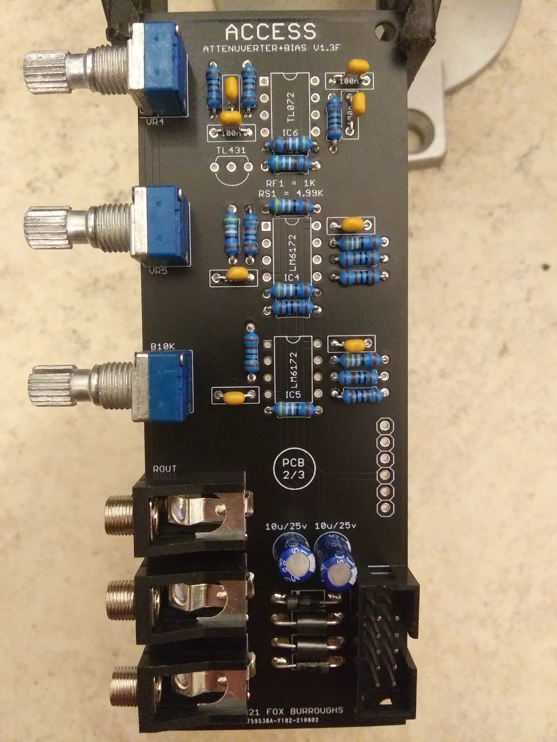
Step 12.
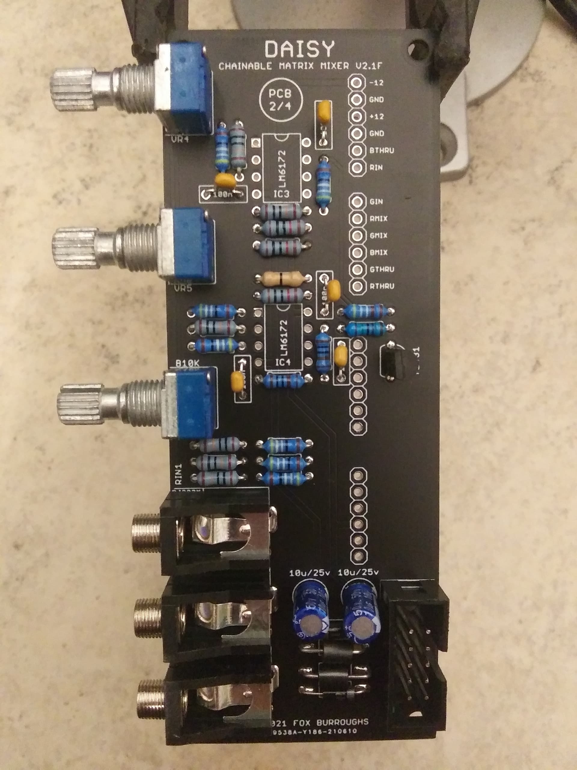
Same as before, we will place each jack and pot into it’s appropriate footprint and then install the loose board into your faceplate. Hand tighten a nut onto each part and make sure they are lined up straight before soldering.
Remove the faceplate.
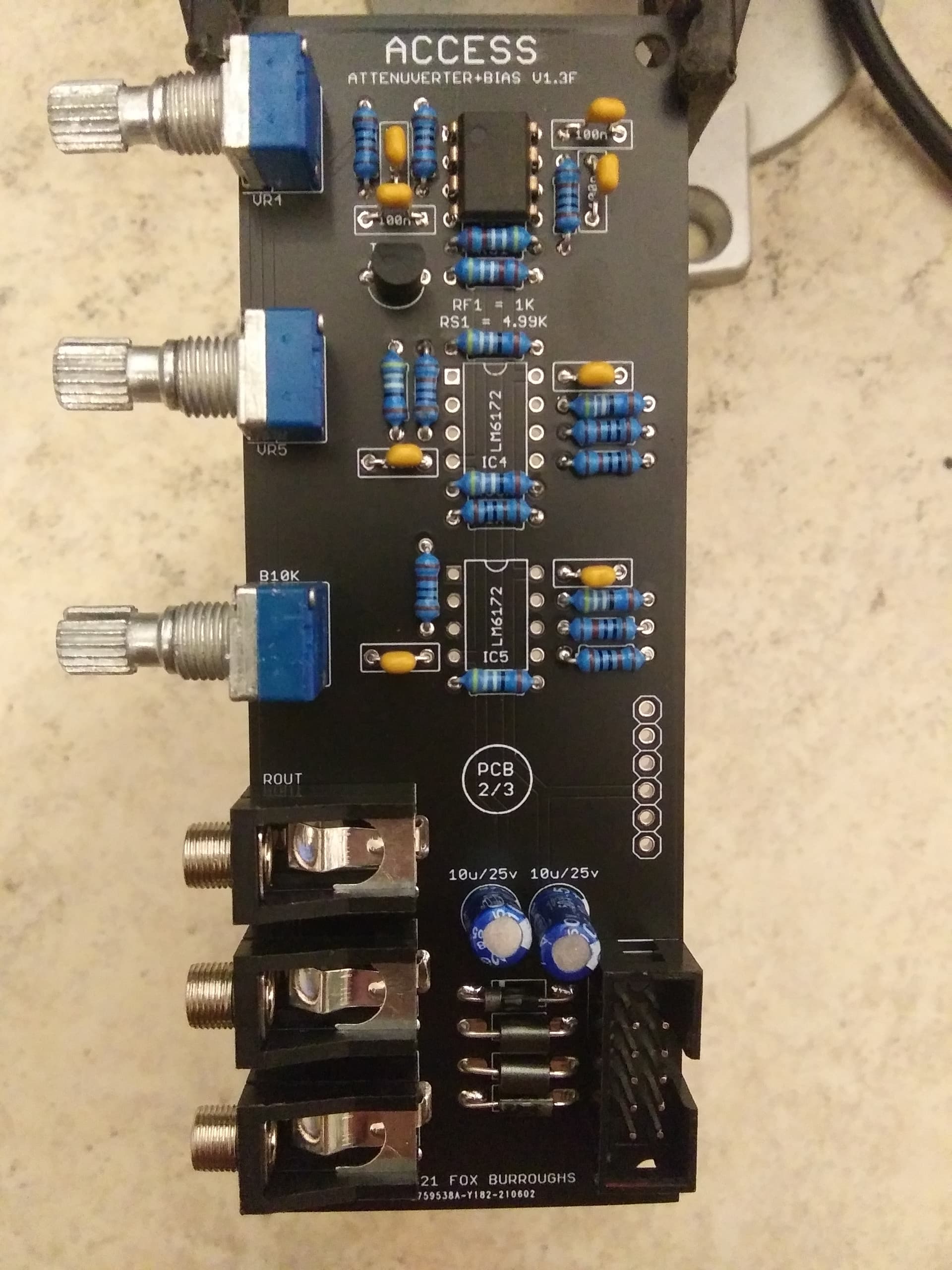
Step 13.
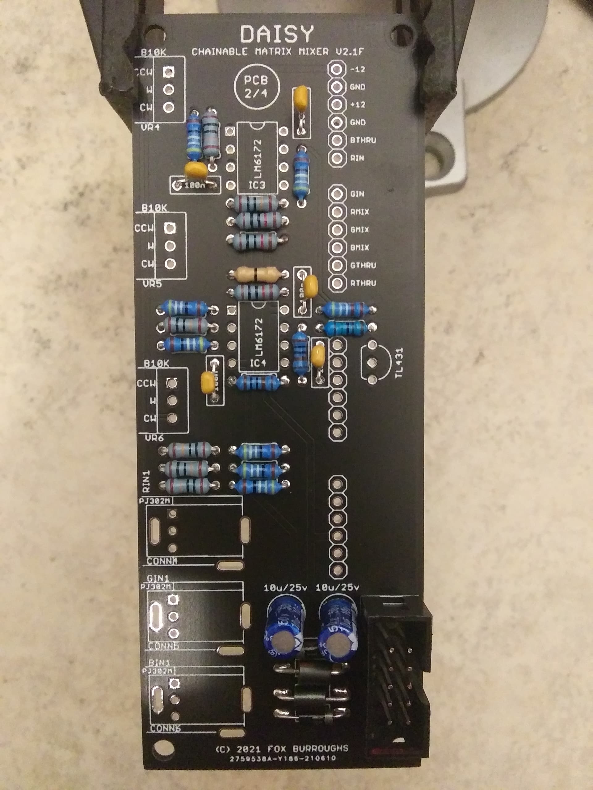
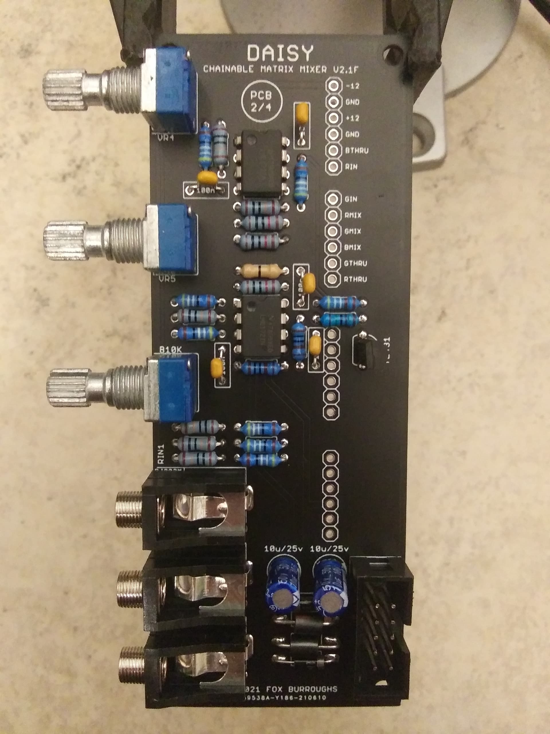
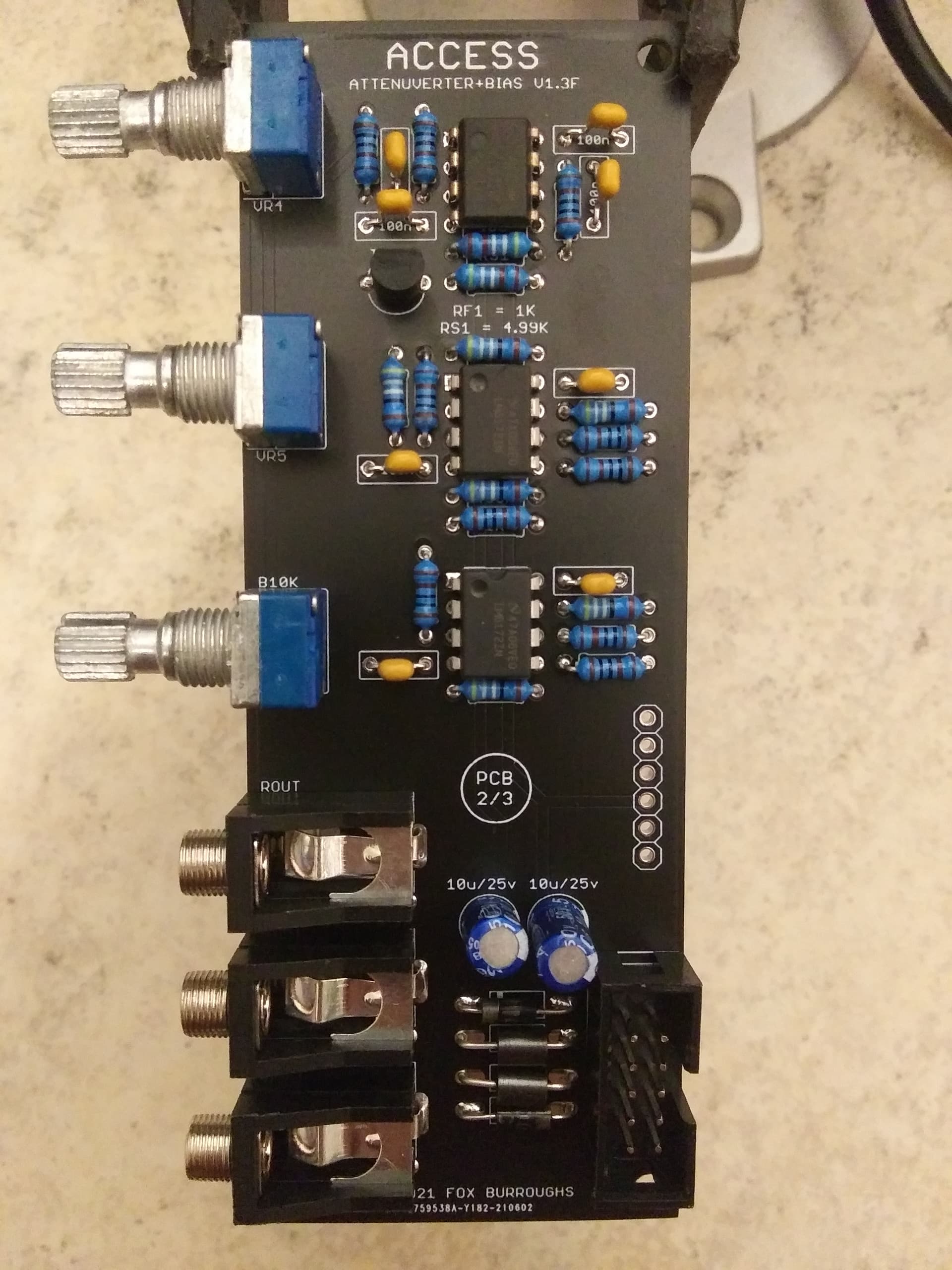
We can finally do the powered semiconductors, namely the TL431 and LM6172’s.
Follow the shape of the silkscreen and line up the flat side of your TL431.
Again, pin one of your LM6172’s can be identified by a dot in it’s plastic encapsulation. Place pin one into the square via for both LM6172’s.
That is all for (PCB 2/4). We can now move on to (PCB 3/4).
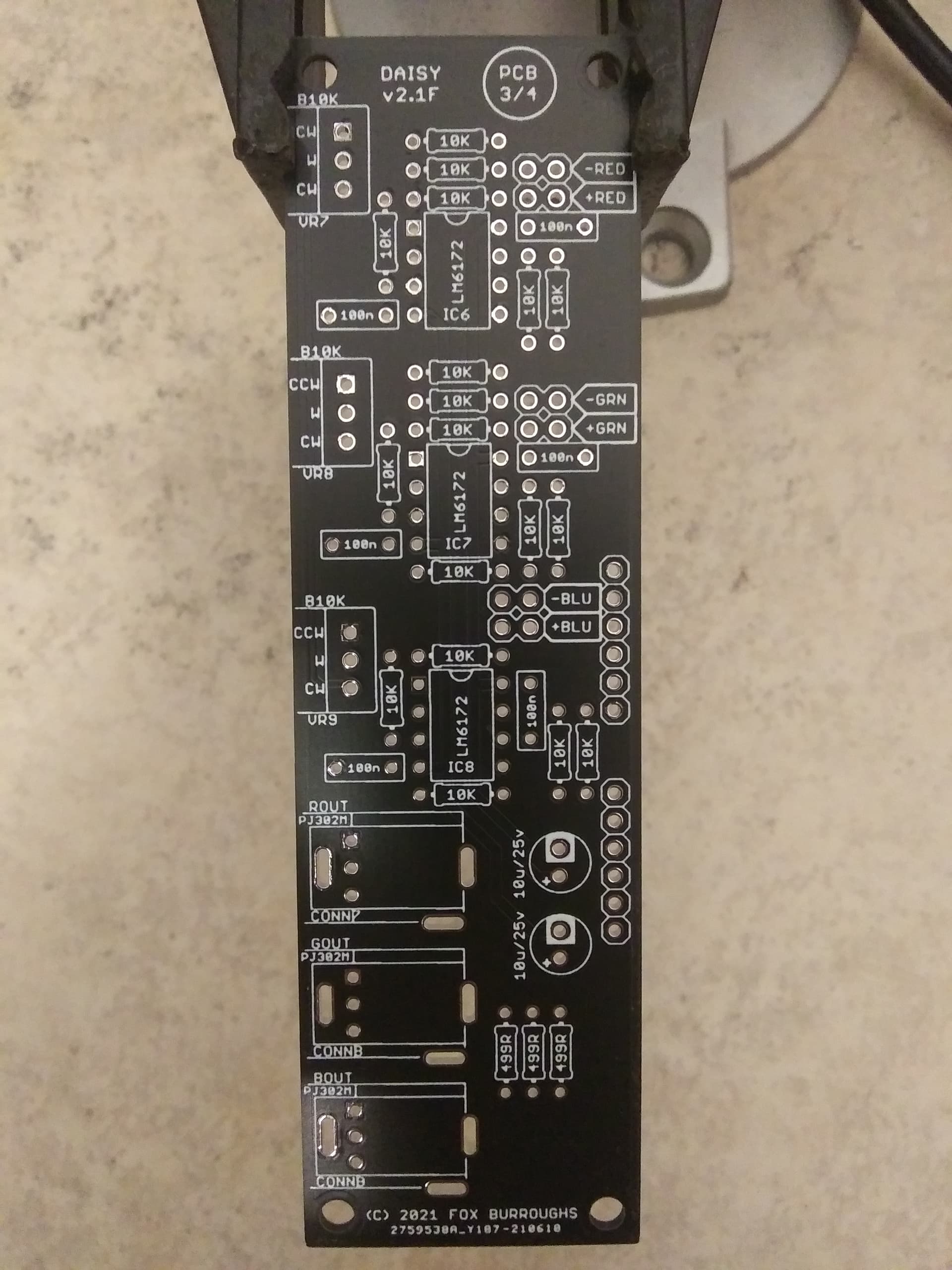
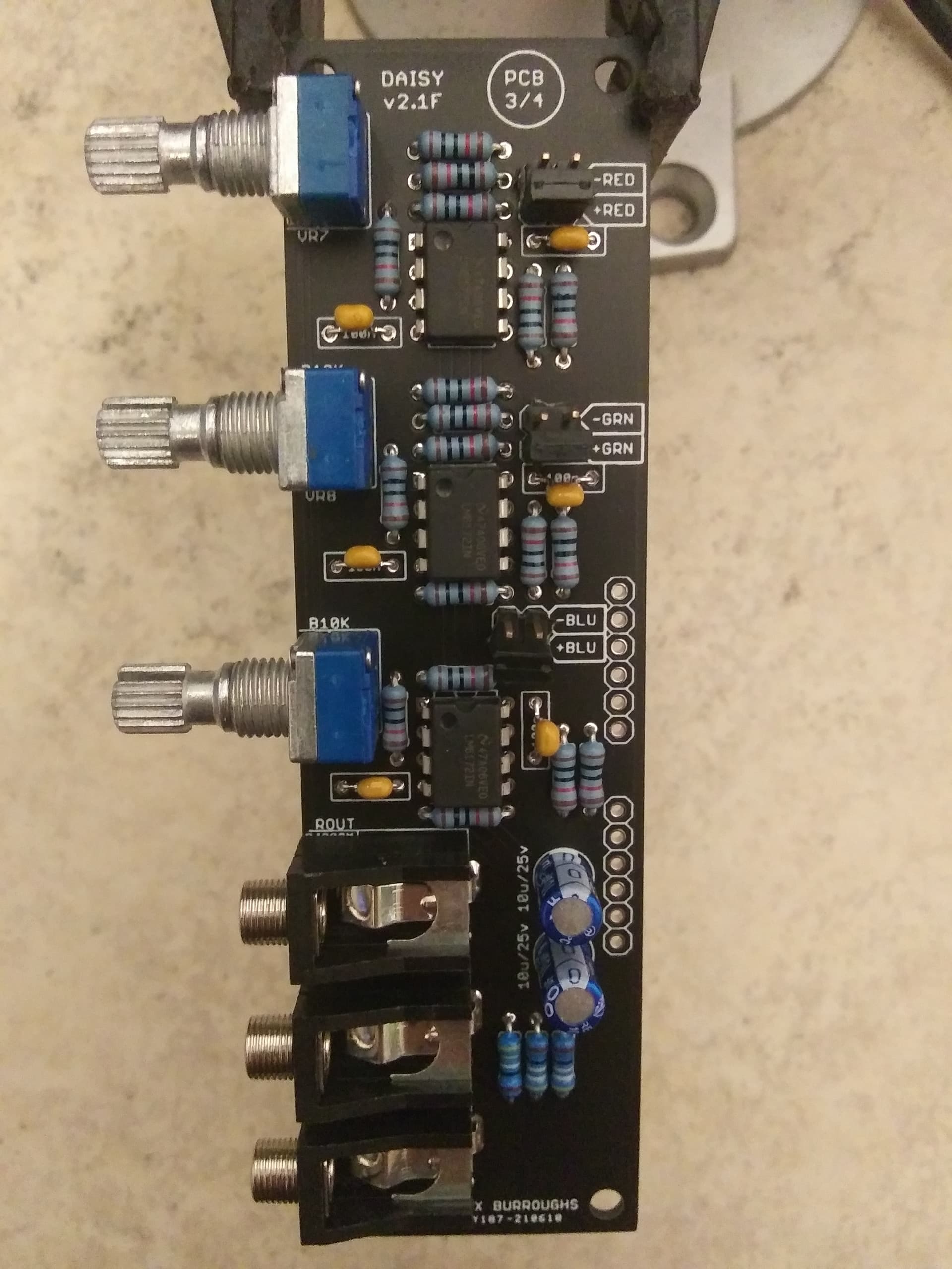
Part 3: DAISY (PCB 3/4)
Step 0.
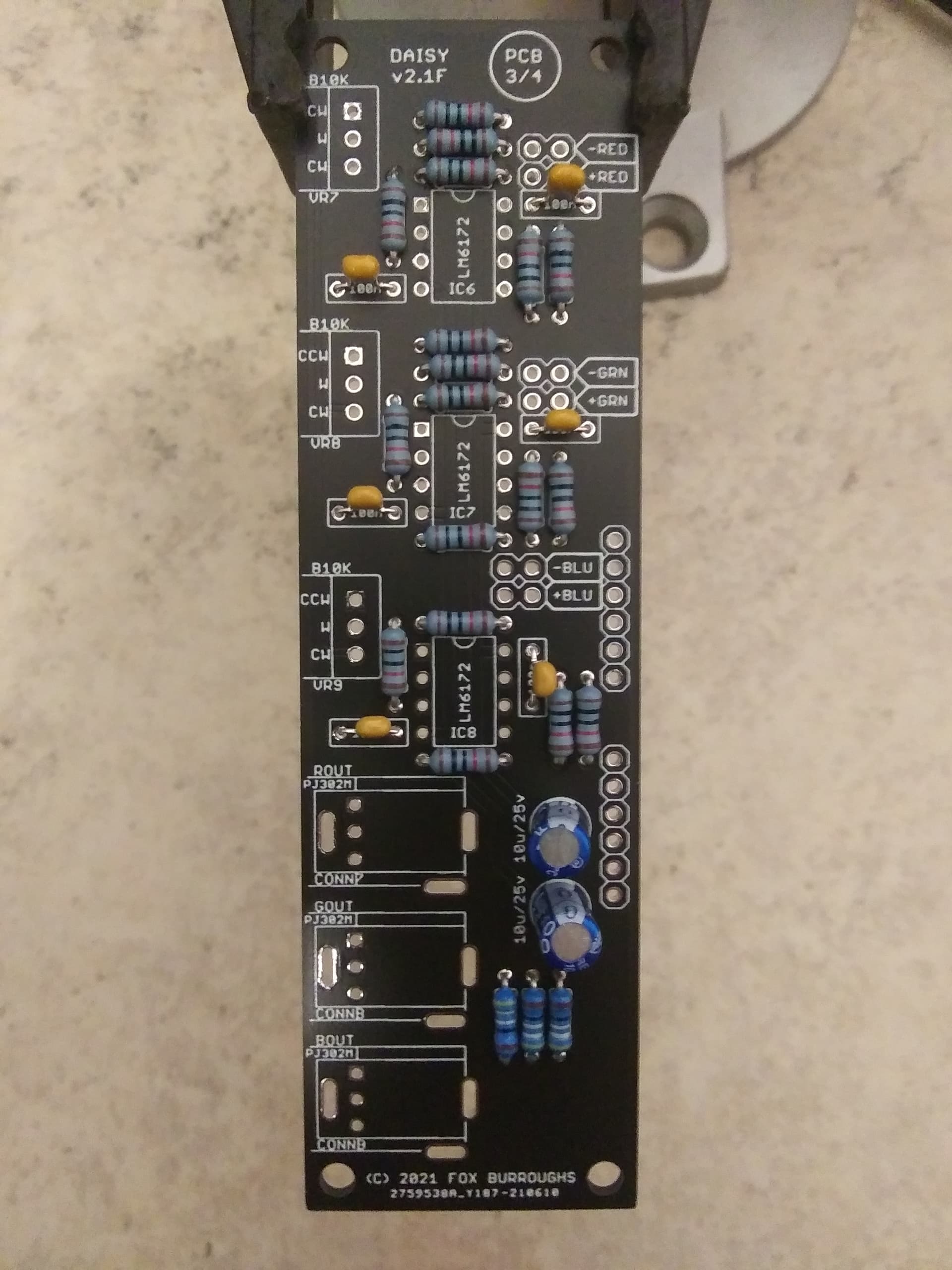
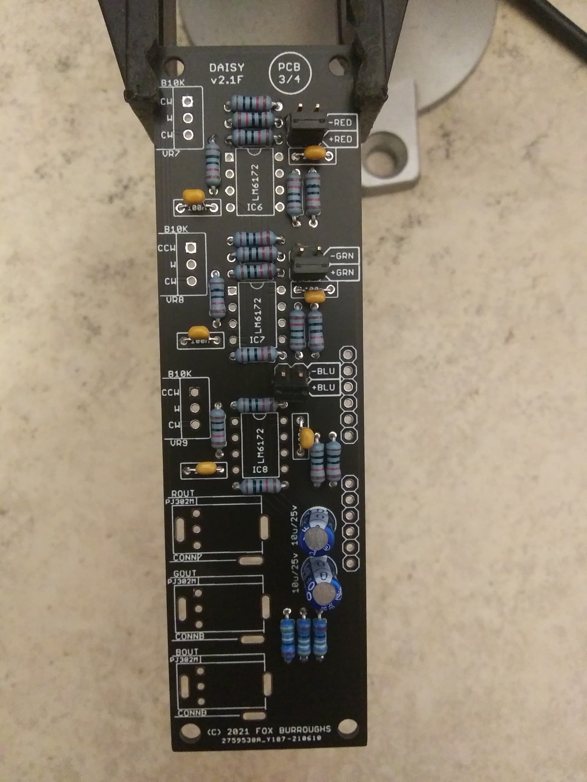
Locate (PCB 3/4) and place t into your vise.
Step 1.
Populate the very last three 499R resistors.
Step 2.
All of the resistors from this point forward are 10K. There are eighteen.
I will solder all of the resistors at this point.
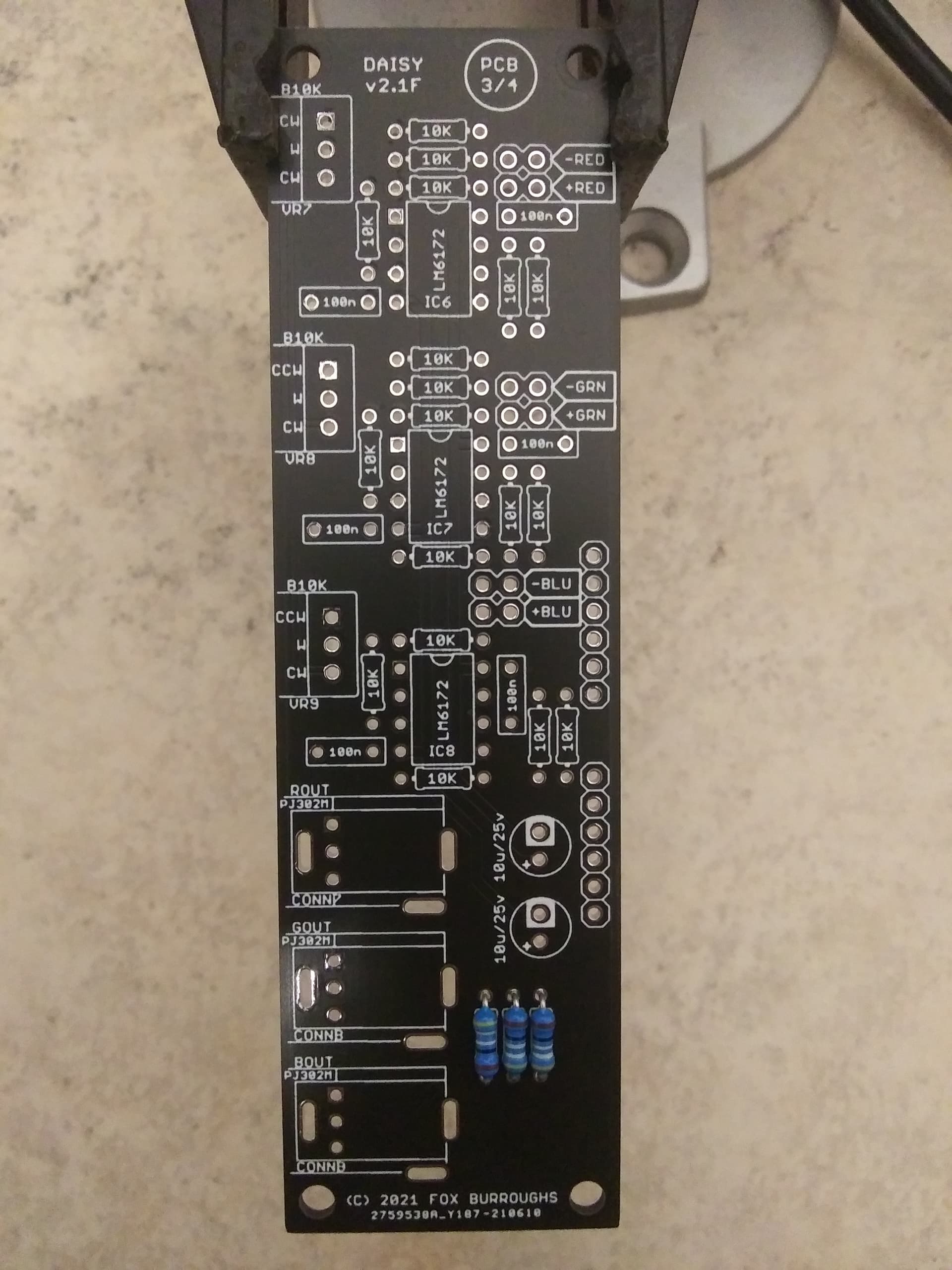
Step 3.
Here we will populate the six remaining 100nF caps.
Step 4.
Two final 10uF electrolytic caps. Line up the negative pins on the board that is outlined in white. Line up the positive pins with the holes marked “+.”
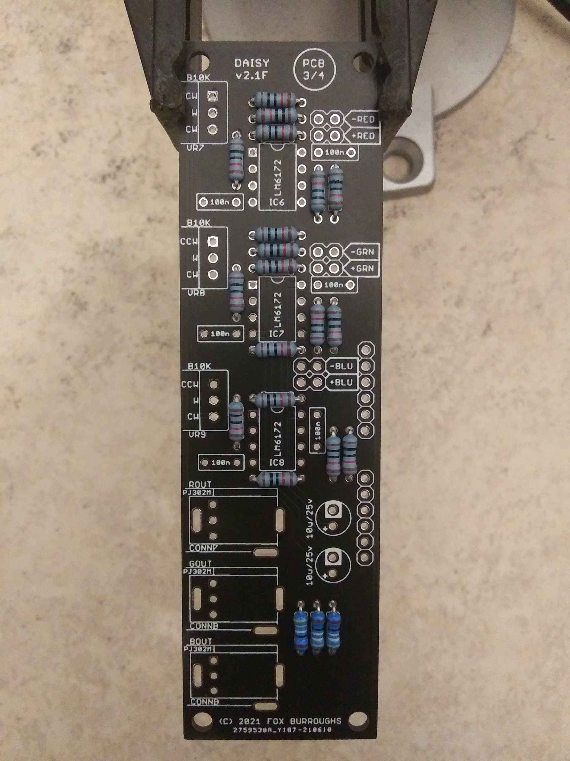
Step 5.
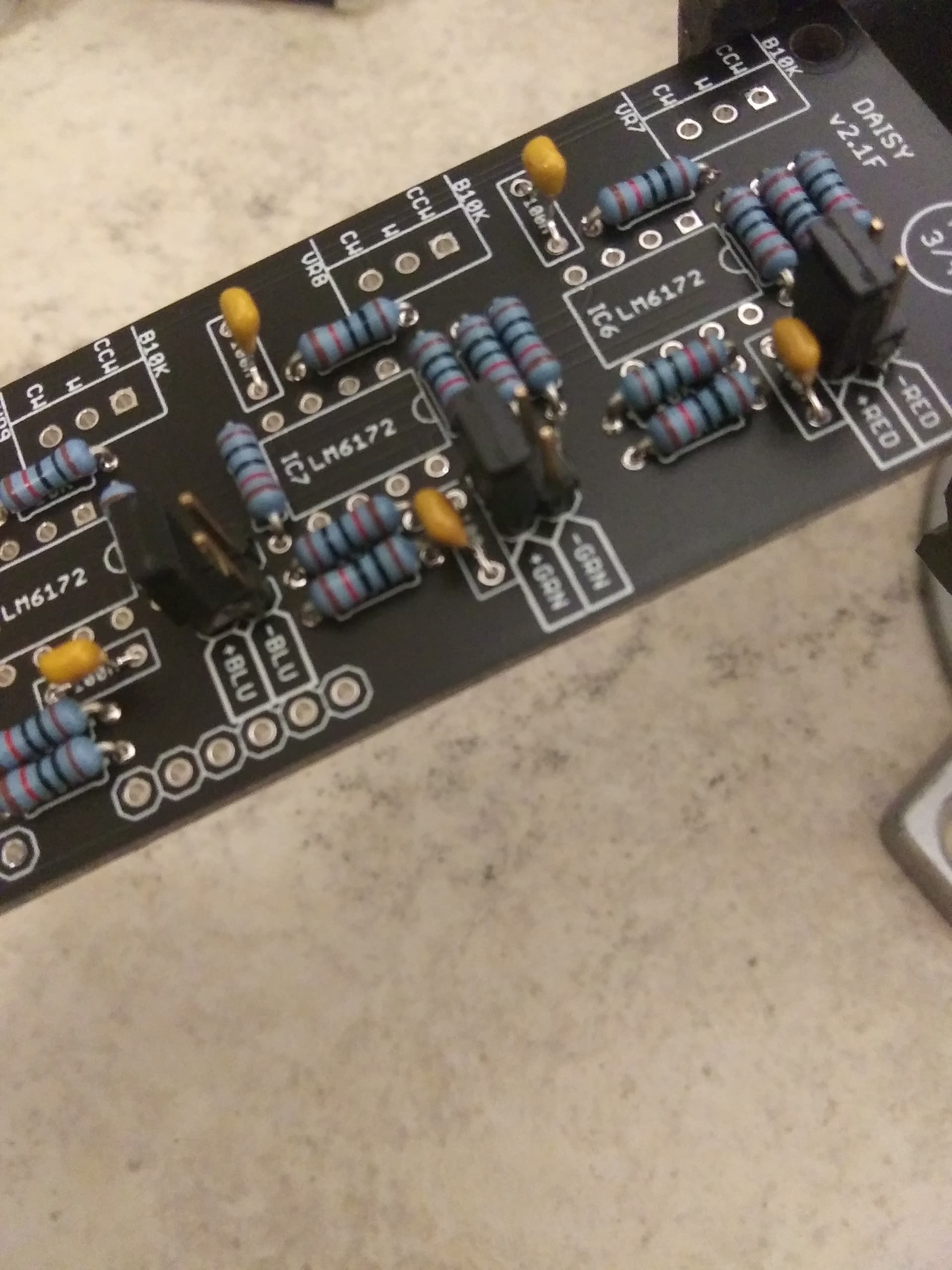
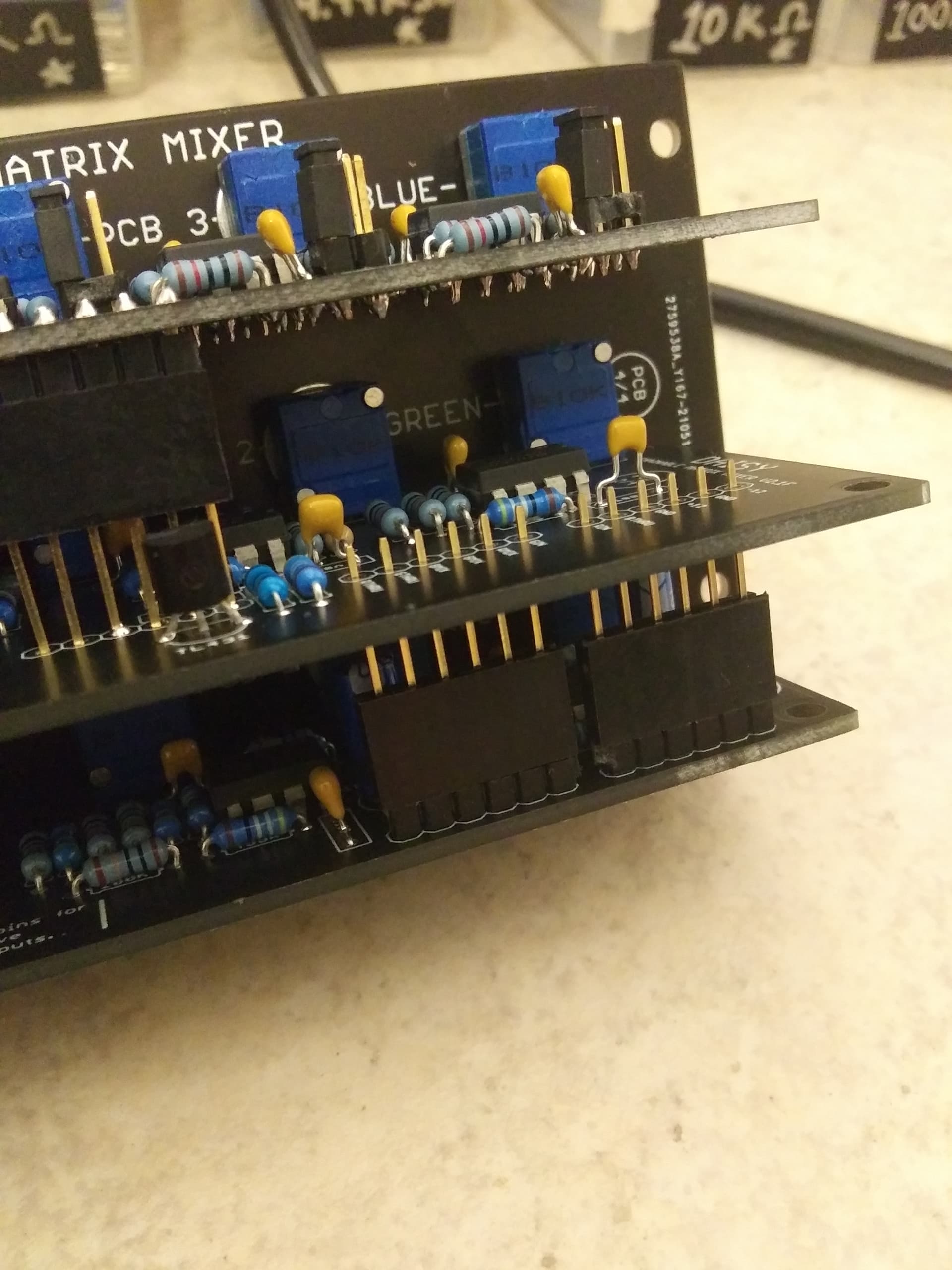
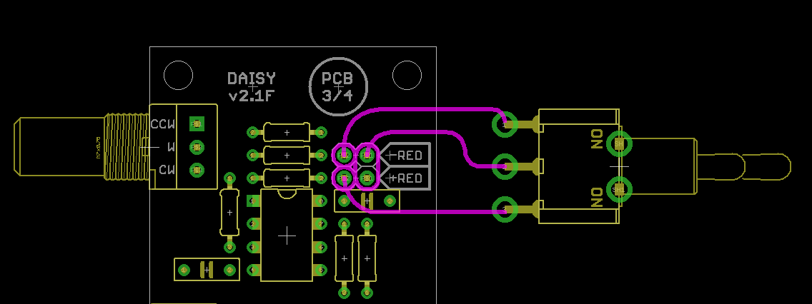
For this step, we need to clip three 2x2 male pin headers. We also need three jumpers, pictured below.
These will be soldered into the three locations labelled [-RED][+RED], [-GRN][+GRN] and [-BLU][+BLU].
Afterward, place your jumpers onto one of the configurations as pictured. Adding a jumper to [-RED] will configure the red CHAIN input to be subtracted from the red output after the matrix.
Adding a jumper to [+BLU] will configure the blue CHAIN input to be added to the blue output after the matrix.
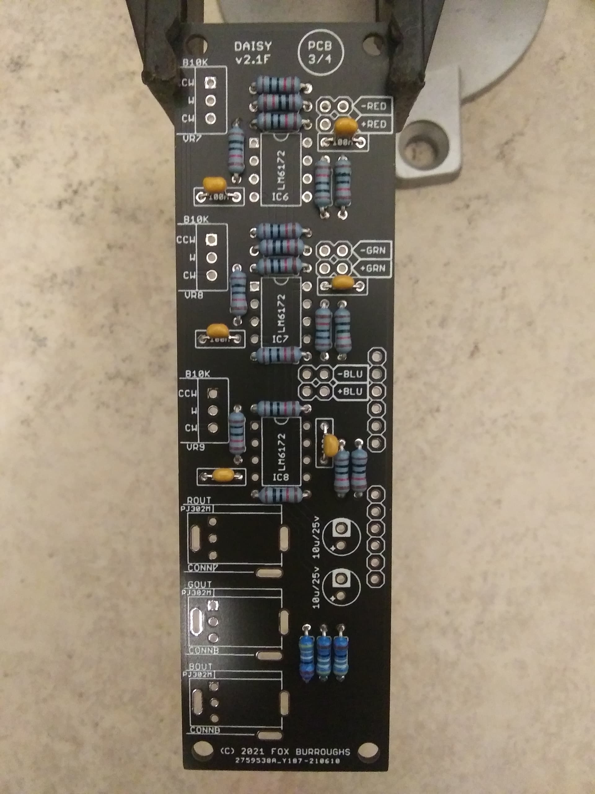
Step 6.
Again, place three pots and three jacks into each f their respective footprints. Place the loose board into the faceplate, and hand tighten nuts to each of them. Once you are sure they are all straight, solder them in place and remove the faceplate.
Step 7.
Now you can solder the last three op amps. All three are LM6172’s and need to be placed into their sockets correctly. Line up pin 1 of each with the square via, indicating pin 1.
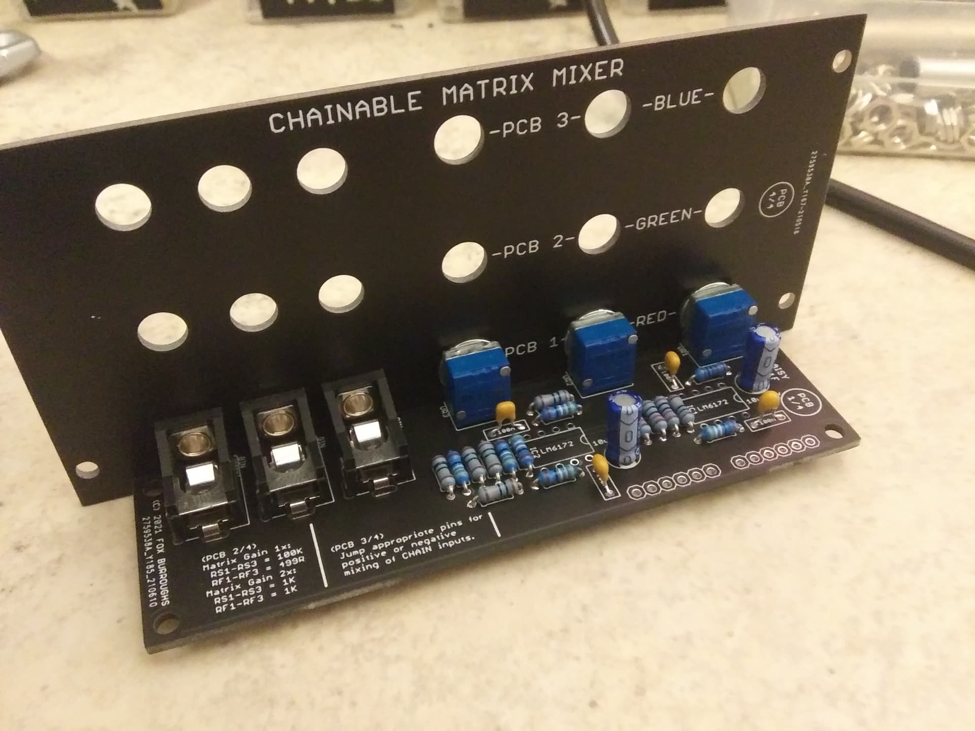
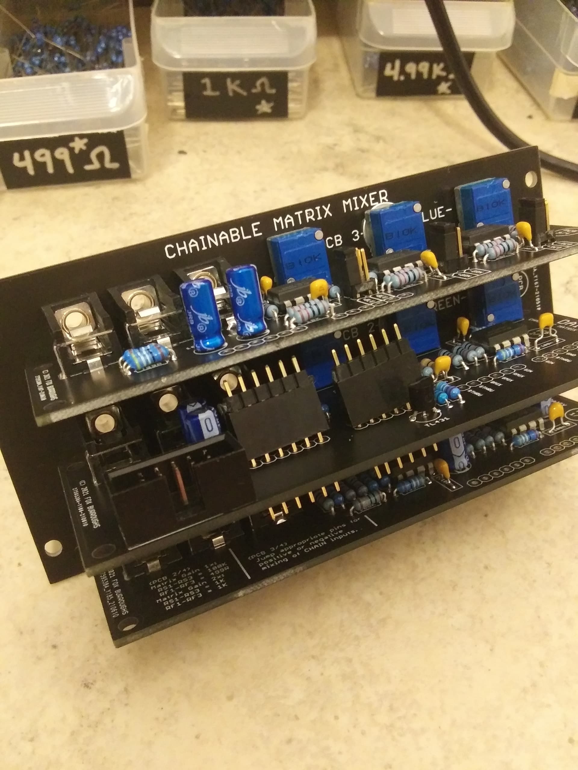
We can now move onto the final part of assembly. Locate (PCB 4/4) which is the faceplate.
Part 4: DAISY (PCB 4/4)
Step 1.
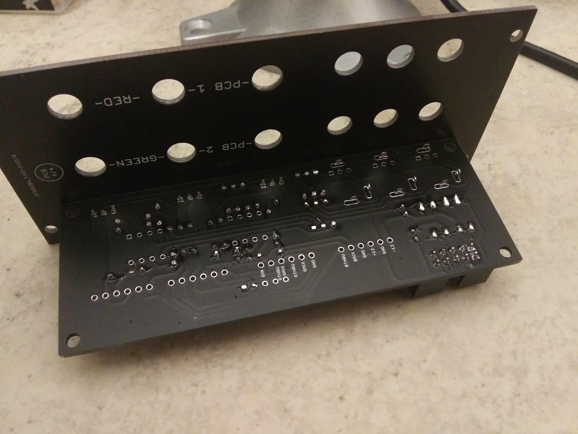
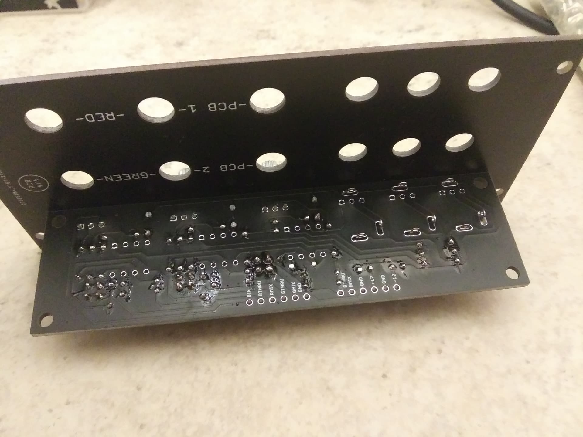
We can finally install all three PCBs into the faceplate. The column marked -PCB 1- is where you will place (PCB 1/4), the column marked -PCB 2- is where you will place (PCB 2/4) and the column marked -PCB 3- is where you will place (PCB 3/4).
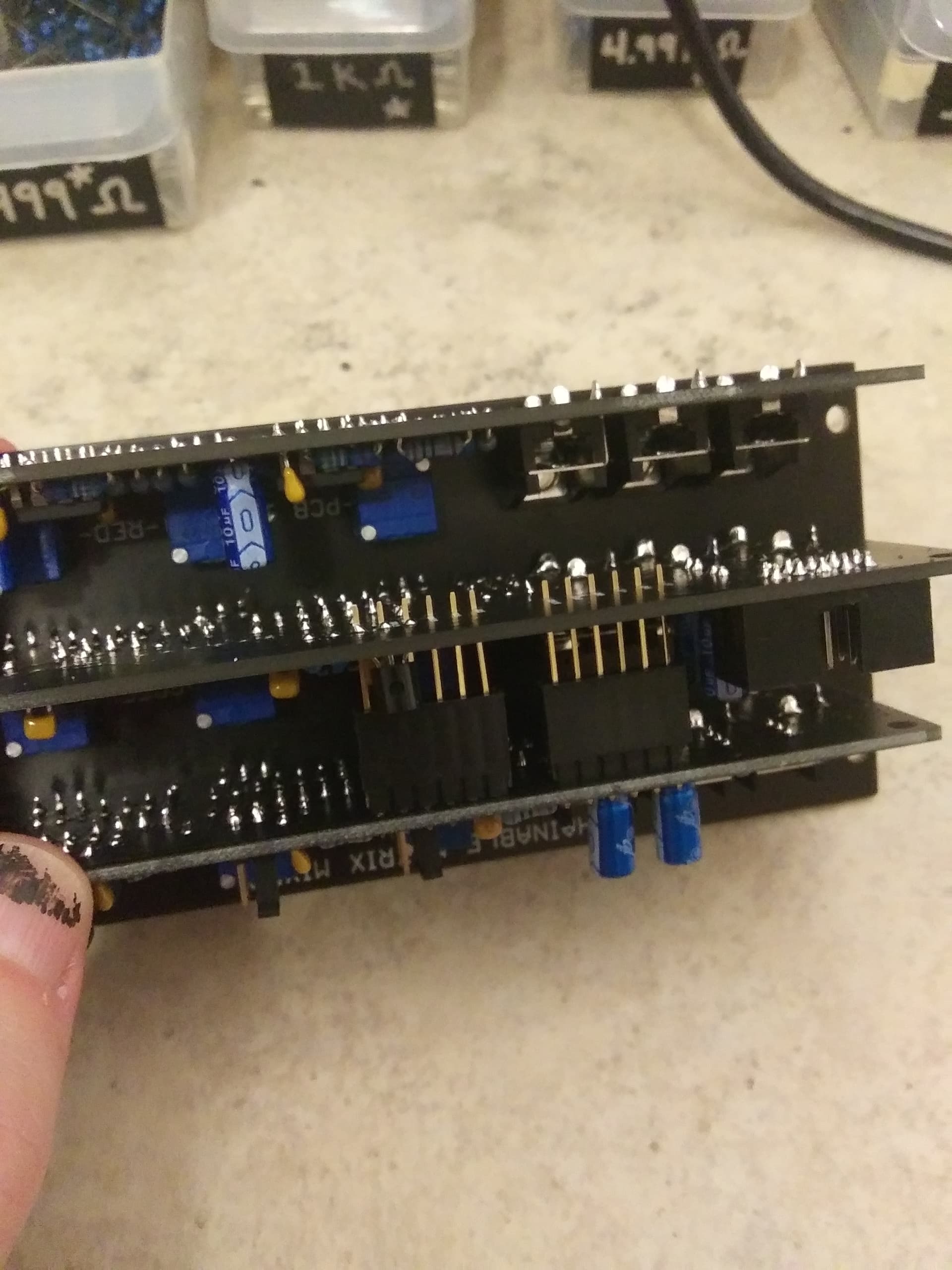
Hand tighten a few nuts onto each board. The pot and bottom jack of each is a good choice.
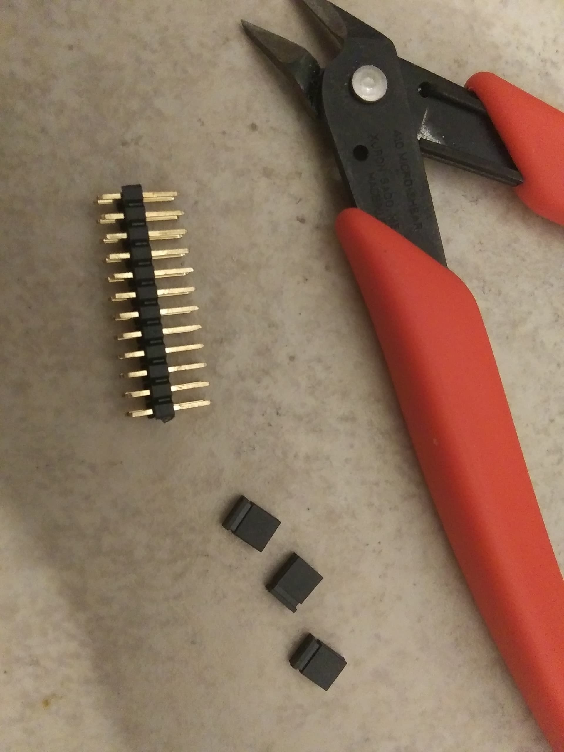
Step 2.
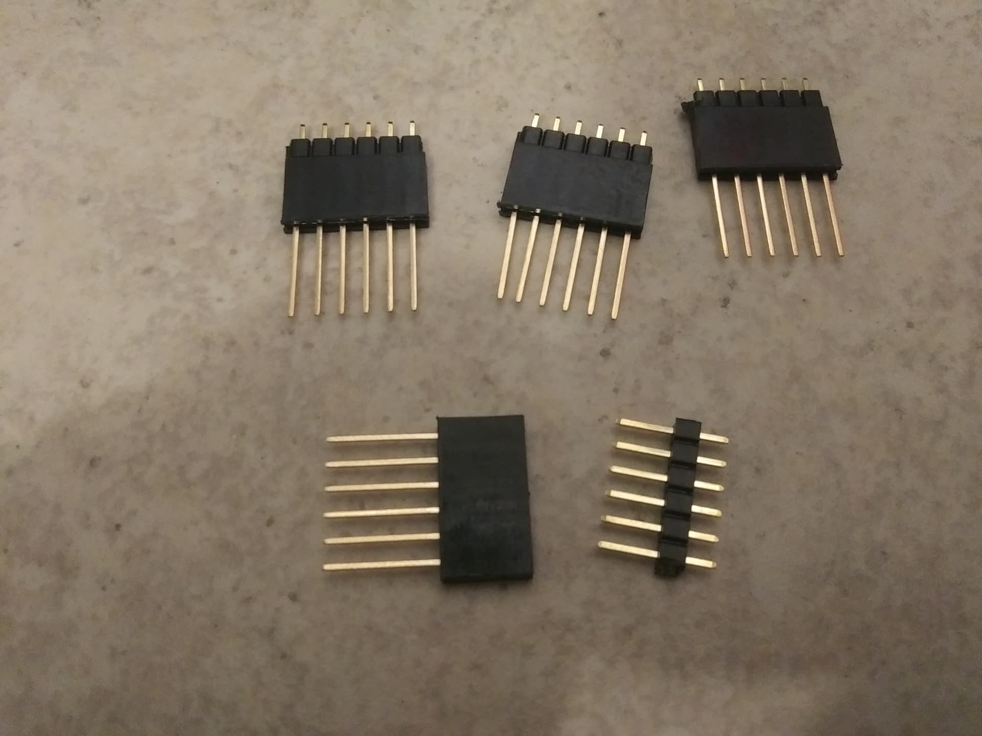
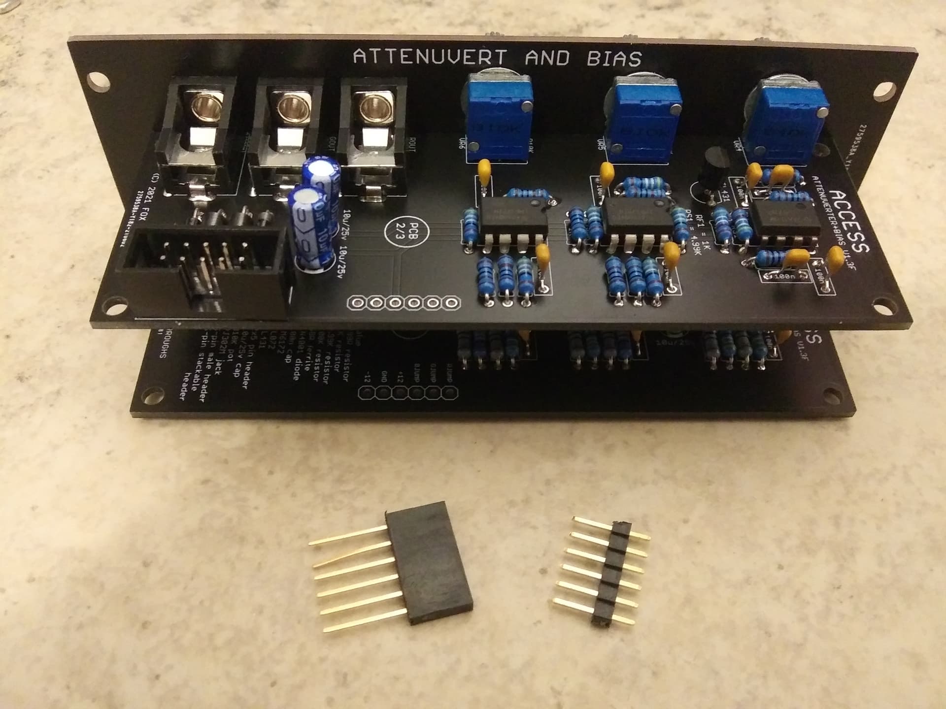
Locate four stackable 6-pin headers and snip four 6-pin sections of male-pin headers.
Put them together a pictured below.
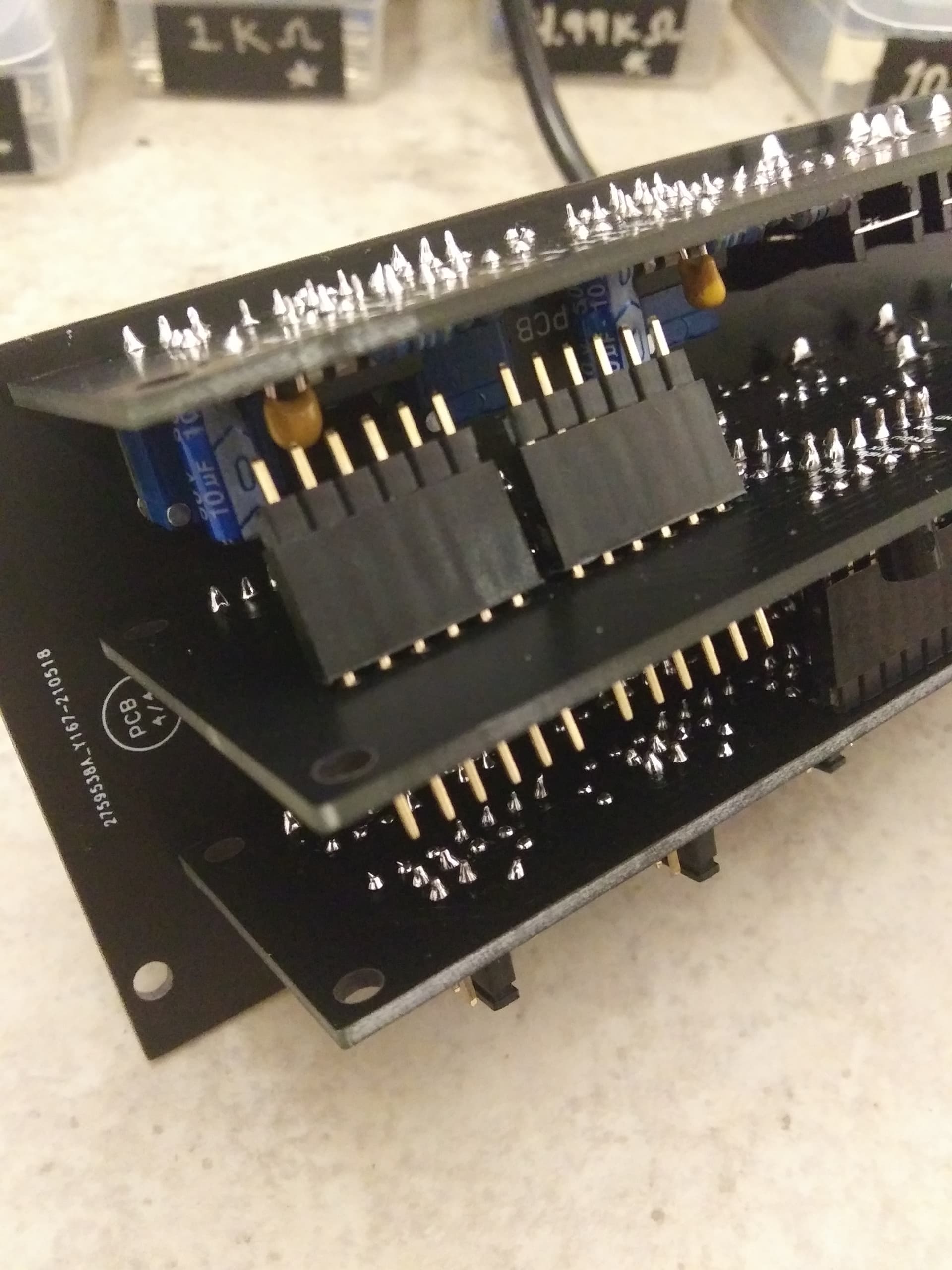
Step 3.
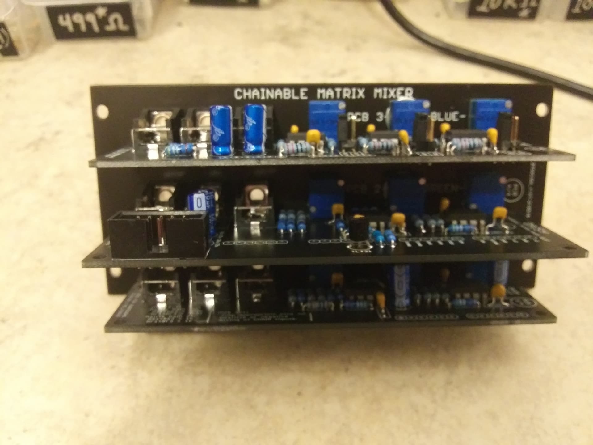
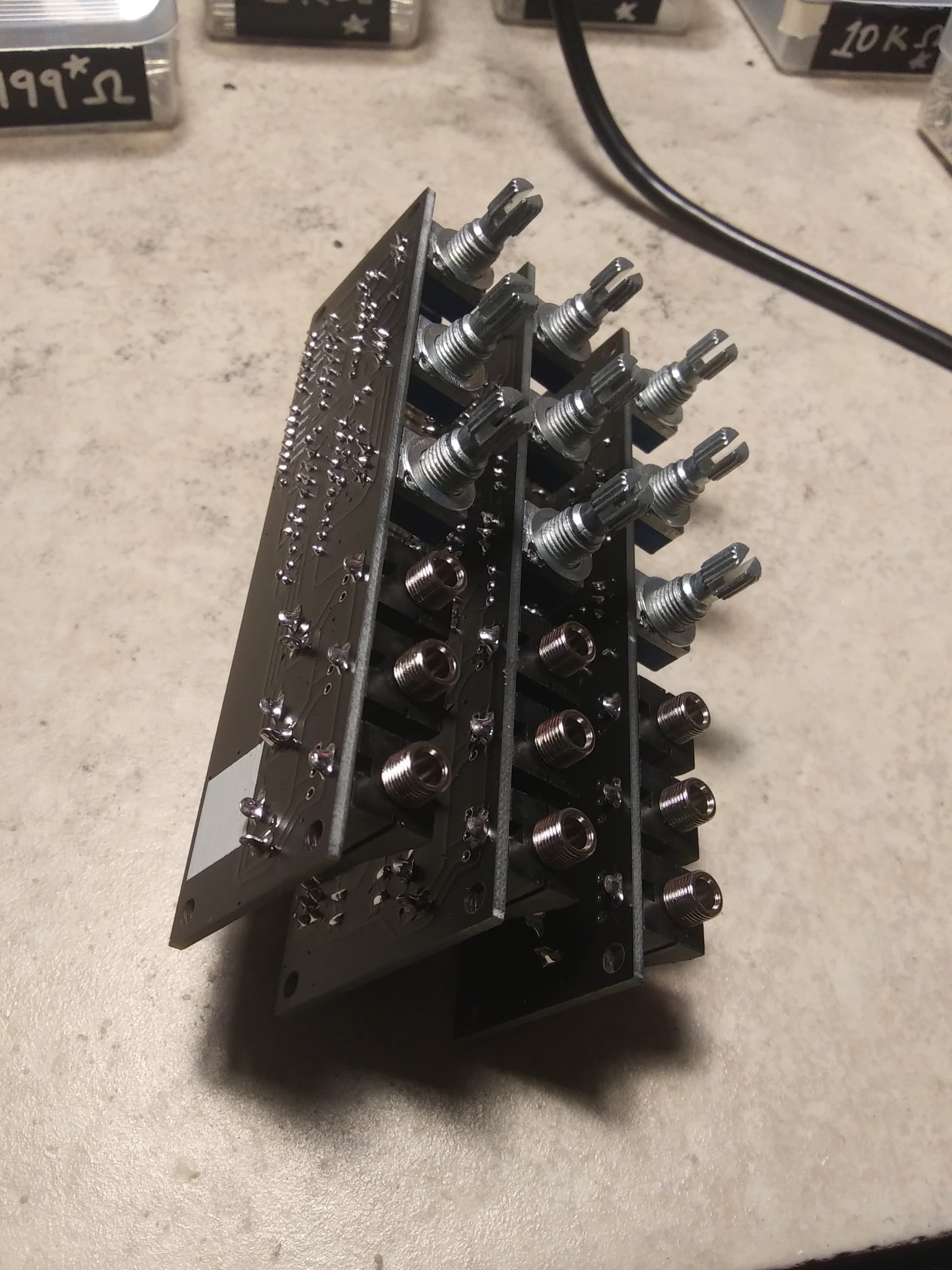
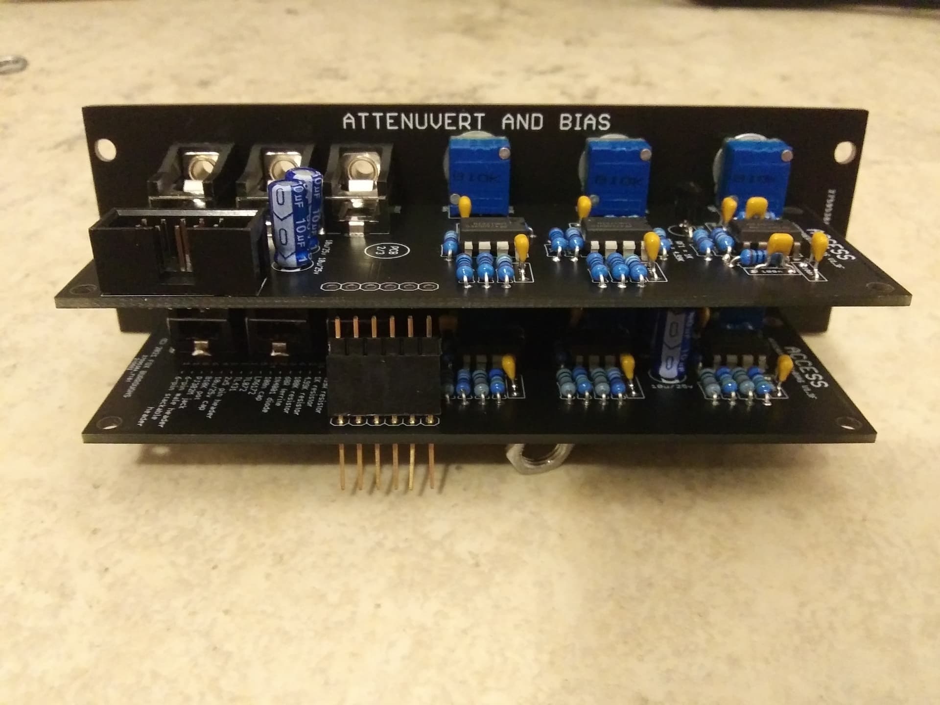
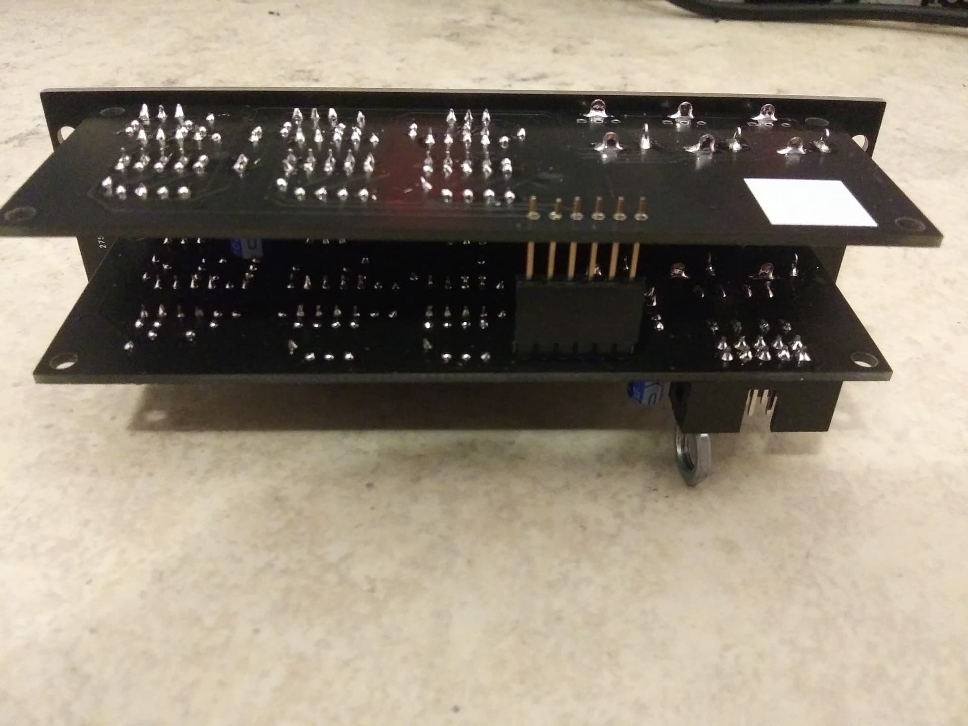
Take two of your stackable headers with the male pins header inserted and place the long-side into the center board. They will fall into the holes. Then turn the module over and they will fall toward the other side. Adjust the headers so that they fall into the other side and solder all 24 pins (that is six-pins times four sides).
Double check your work and make sure all of the pins are soldered.
Step 4.
This is the same as step 3, but we will place the two remaining headers into the two remaining locations. It is easiest to place the long sides of both headers into the center PCB. As pictured.
Then turn the module over and adjust the header so that the opposite pins fall into the correct holes.
Solder all 24 pins and double check that none were missed.
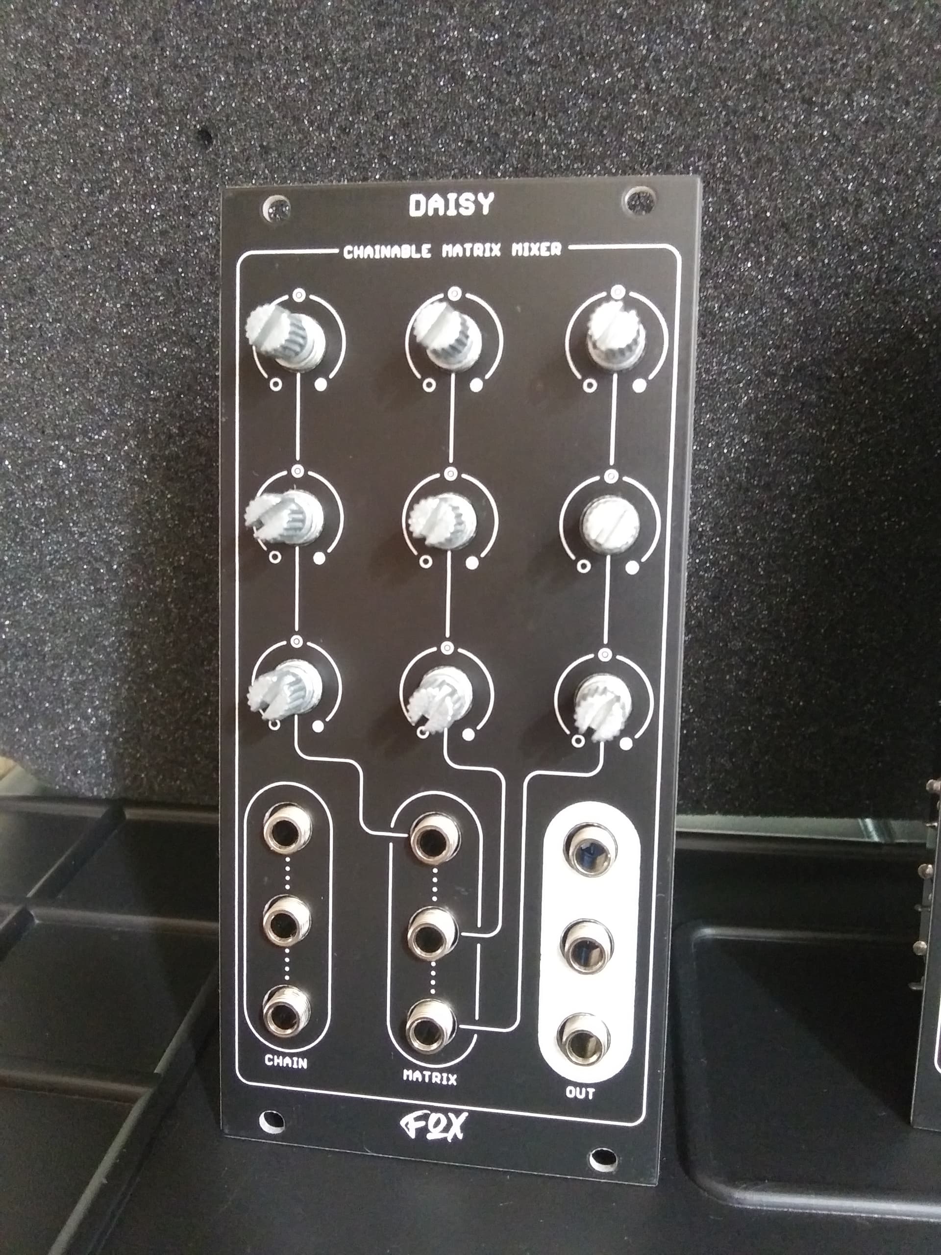
Step 5.
You’re finally finished soldering! At this point, you may take the faceplate off to clean all of your burned solder flux. The boards are connected and very rigid. You may easily disconnect all three boards from each other for this step.
Cleaning your boards allows for you to see any stray solder blobs or cold-solder joints.
Step 6.
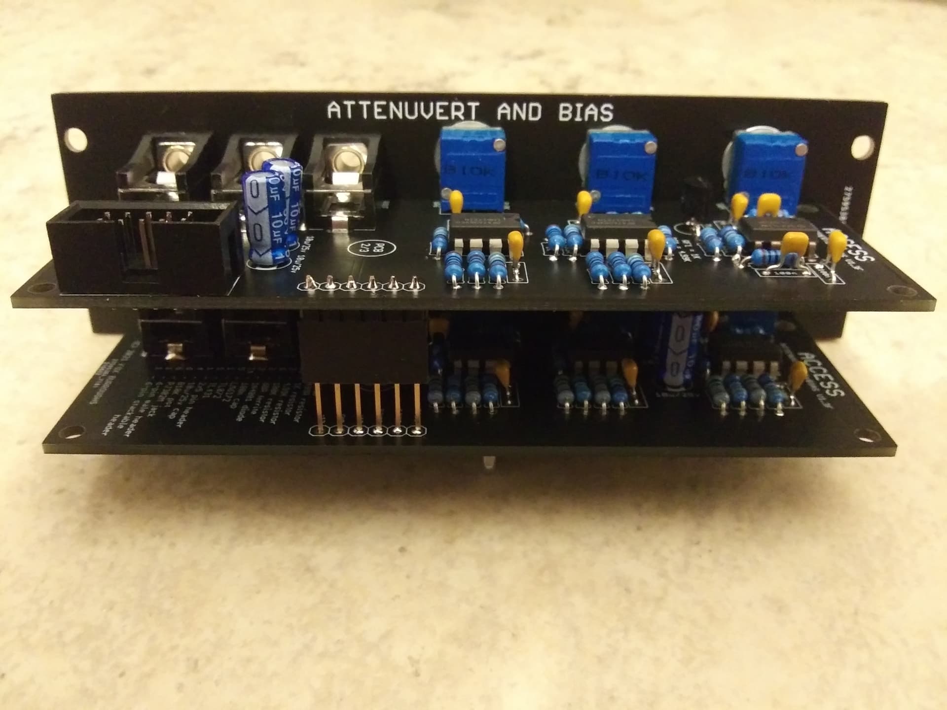
At long last, we may finally reconnect all three boards together and install them into the faceplate.
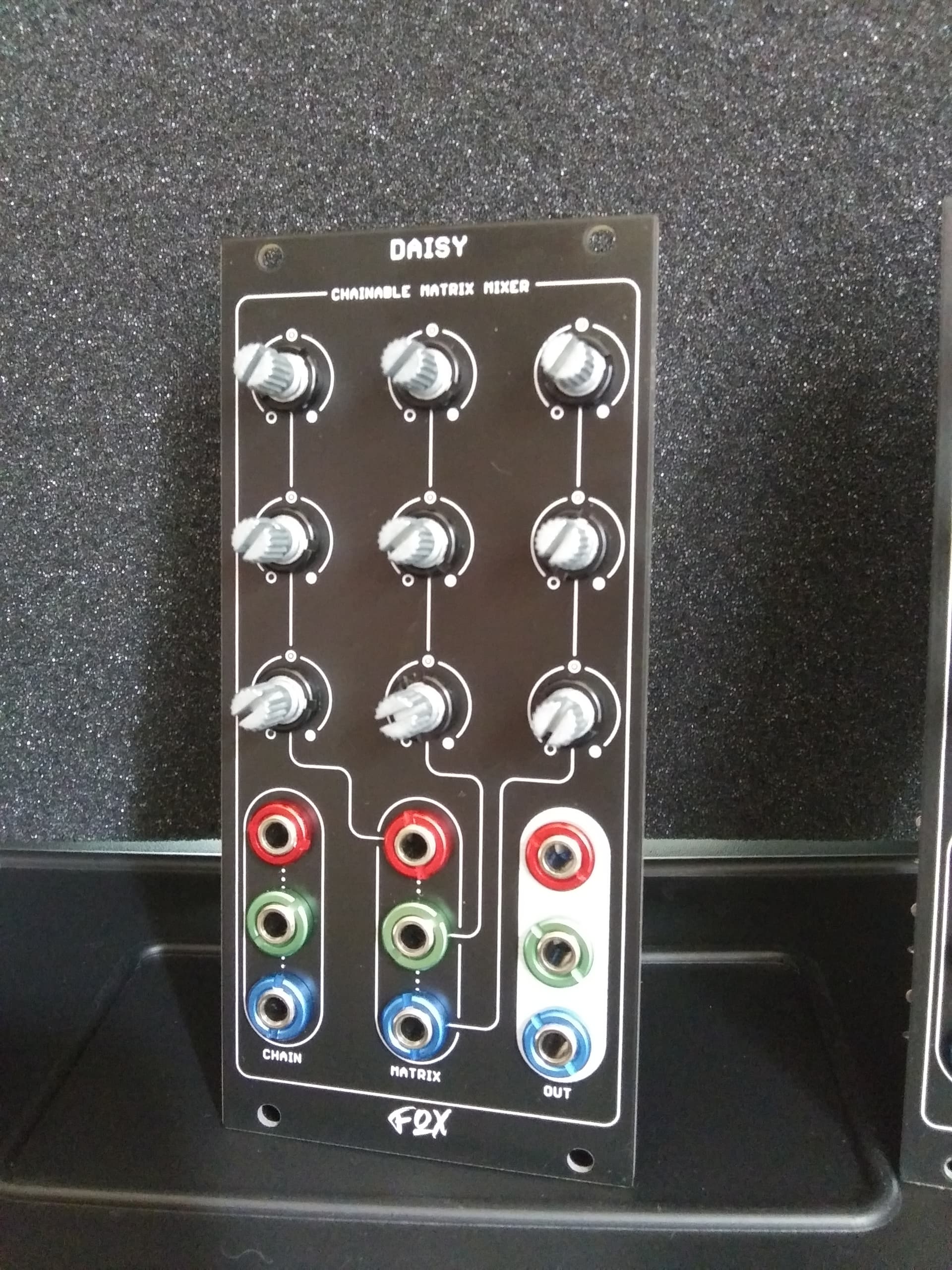
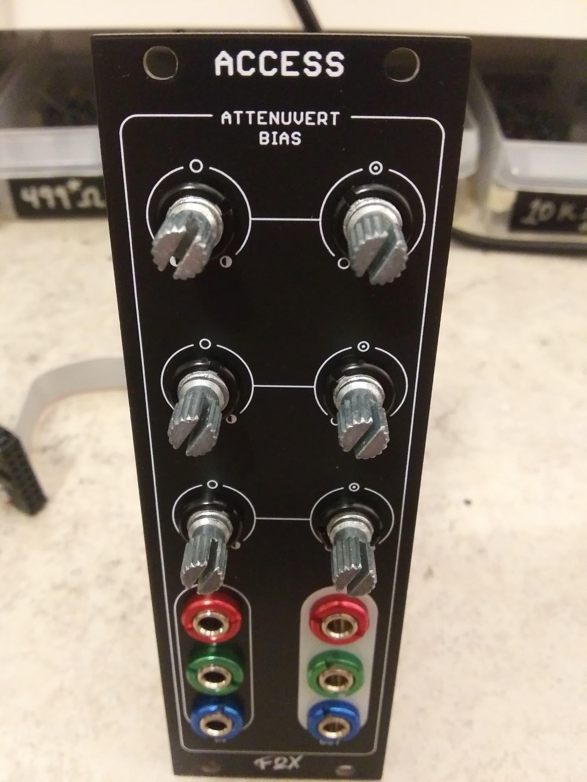
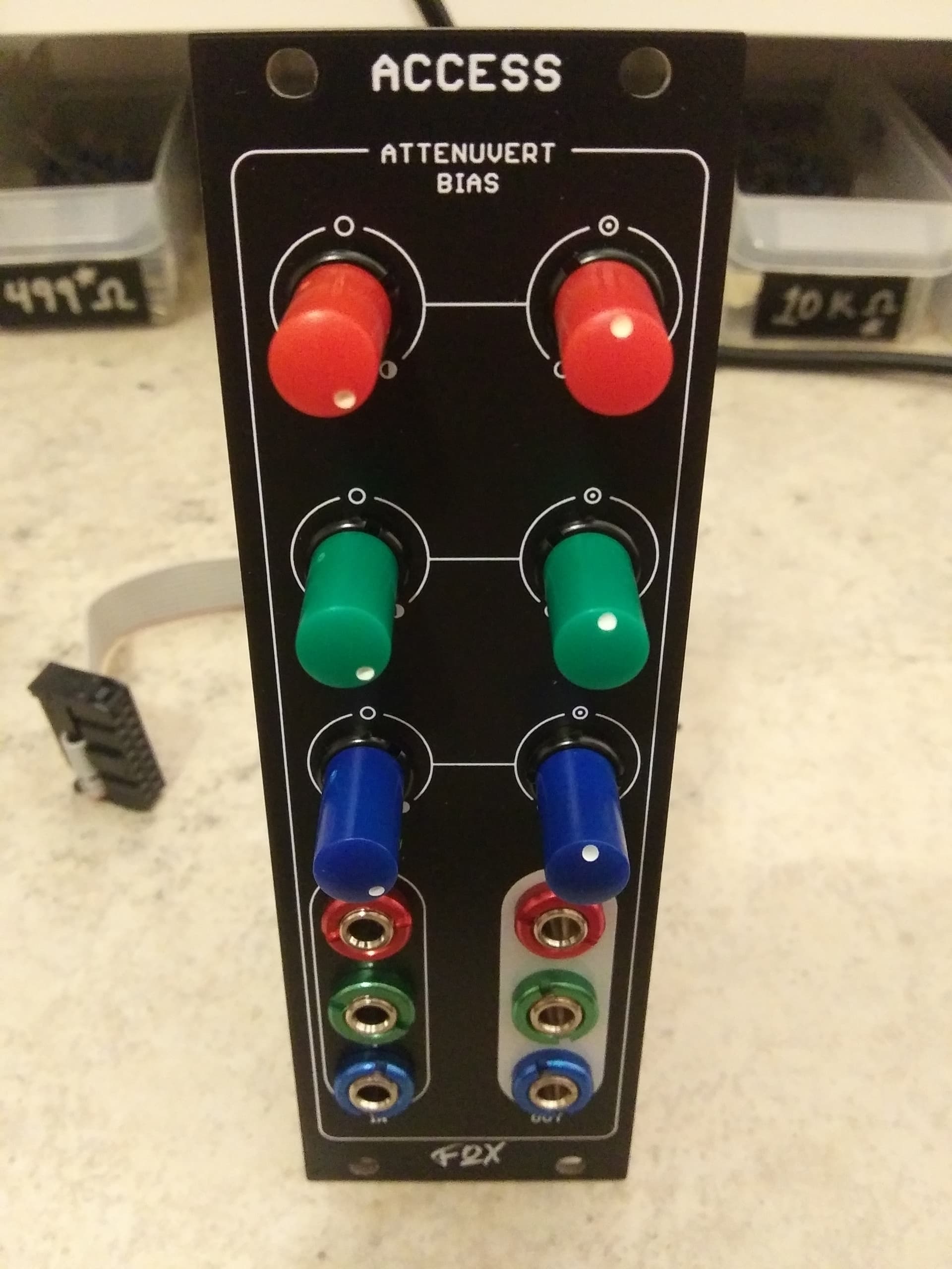
With your Befaco bananut tool, install nine black pot-nuts onto all nine pots.
Install three red bananuts across the top row of jacks.
Install three green bananuts across the center row of jacks.
Install three blue bananuts across the bottom row of jacks.
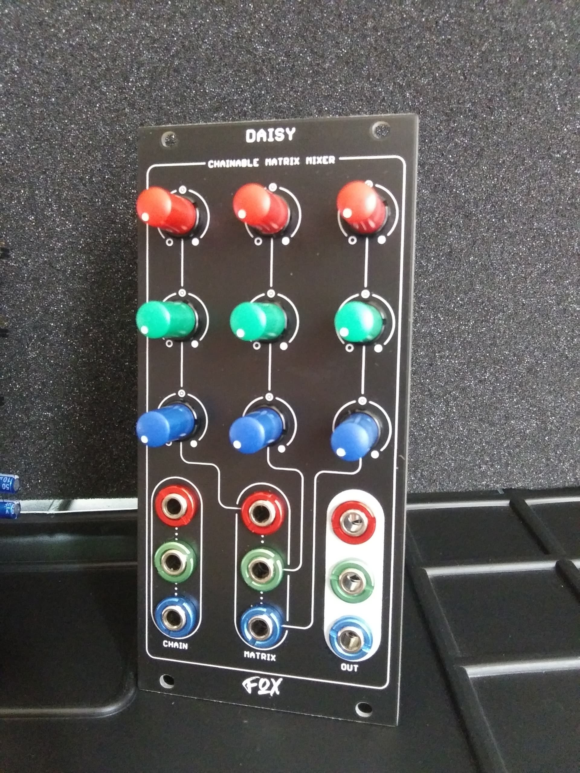
Then locate three red-, three green- and three blue- micro knobs. Turn all 9 pots CCW so that the slot points toward the empty circle on the faceplate’s silkscreen. Take care when placing each knob so that the white dot lines up with the empty circle.
Place three red micro knobs onto the top row of pots.
Place three green micro knobs onto the center row of pots.
Place three blue micro knobs onto the bottom row of pots.
At this point (believe it or not) you are ready to hook up a power ribbon cable and rack the module to test. Plug in some luma sources and start colorizing!