Currently under construction. Almost finished.
If you are having difficulty choosing a configuration for your A+B-C module, I recommend (A+B)/2-C.
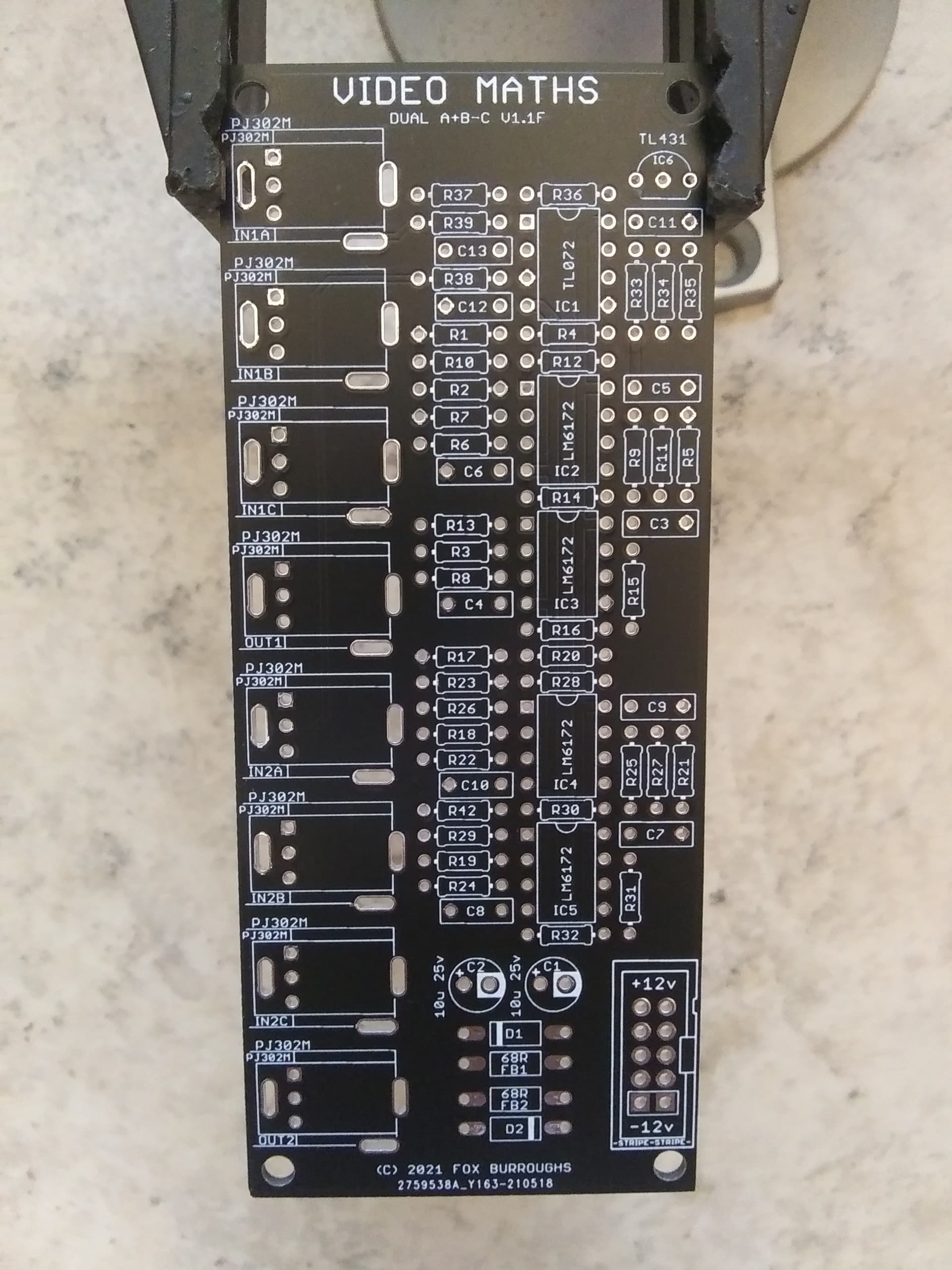
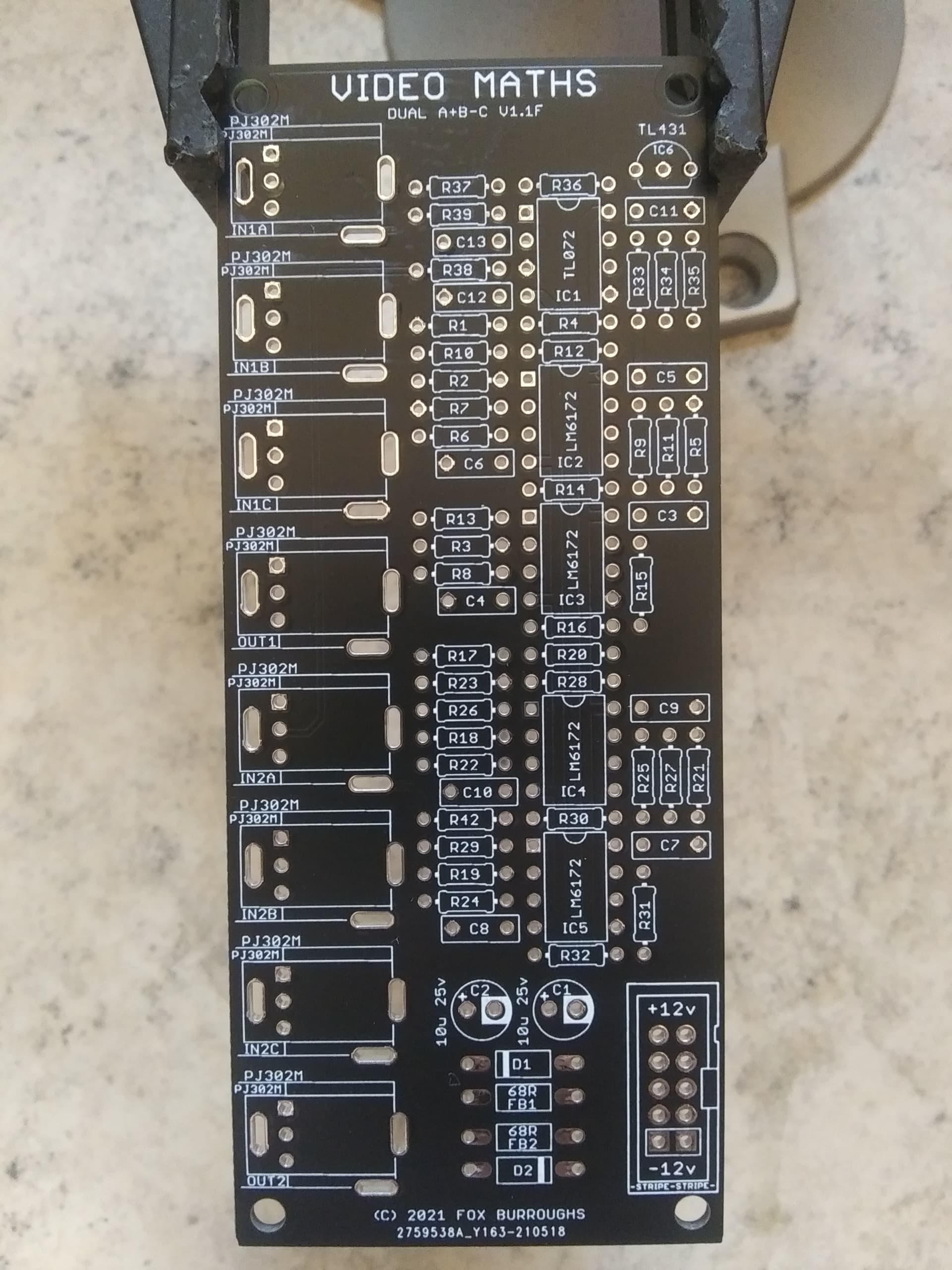
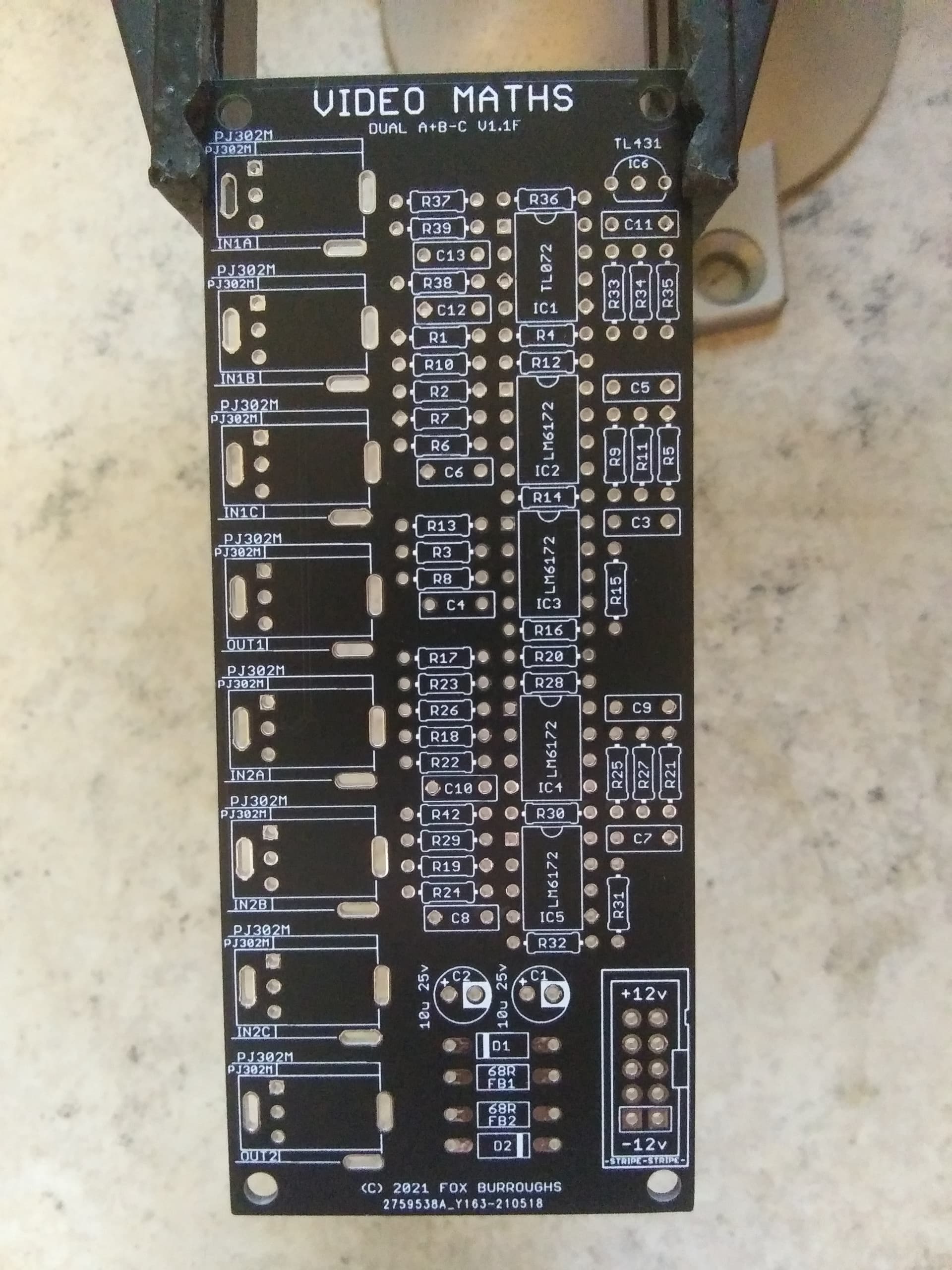
BOMs and Build Guides
BOM for A+B-C configuration
| Qty | Value | Parts |
|---|---|---|
| 1 | 10-Pin Box Header | CONN9 |
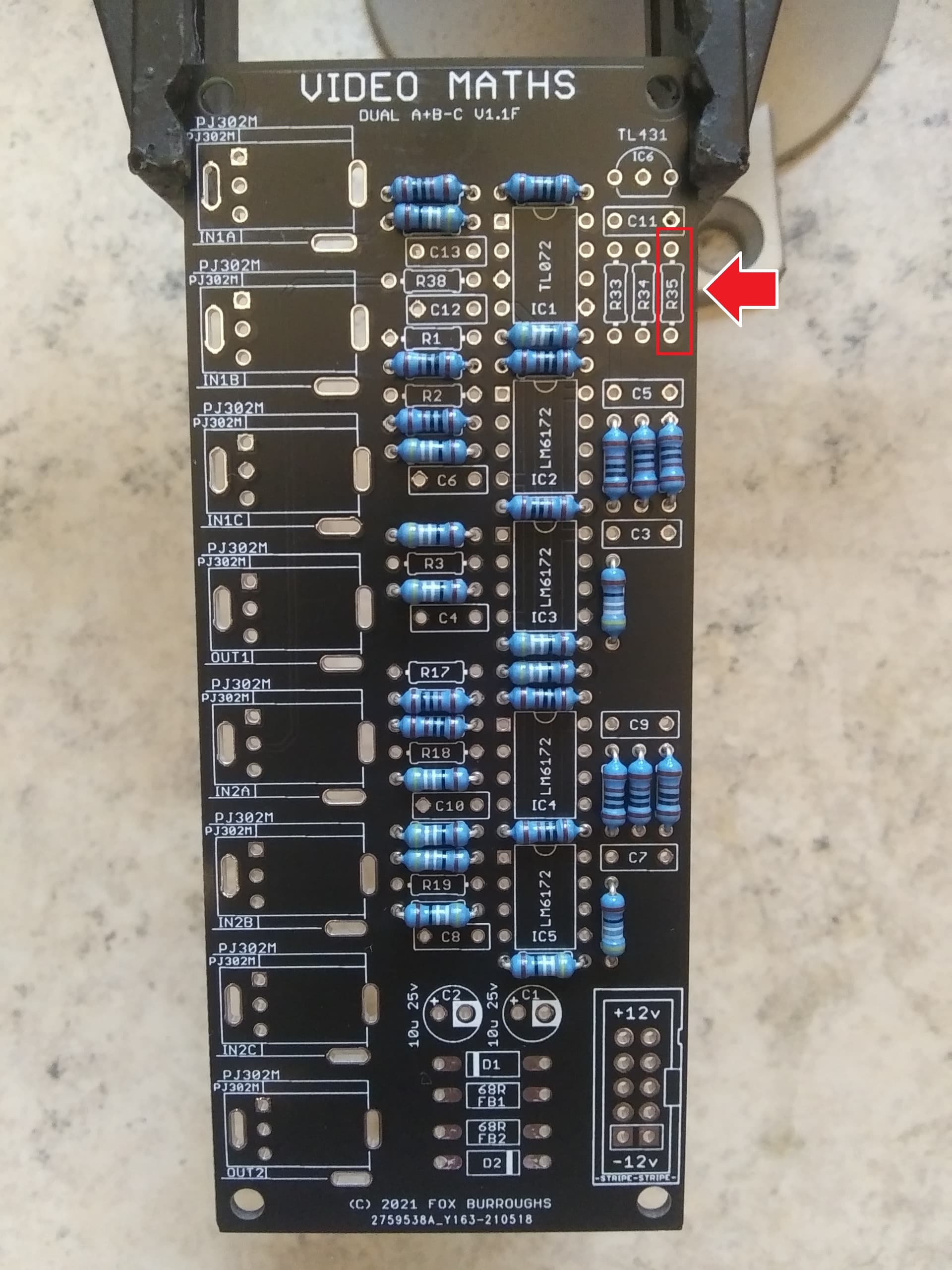
| 1 | 2K resistor | R35 |
| 1 | TL072 IC | IC1 |
| 1 | TL431 reference | IC6 |
| 2 | 10u/25v capacitor | C1, C2 |
| 2 | 1N4001 diode | D1, D2 |
| 2 | 4.99K resistor | R33, R34 |
| 2 | 68R ferrite bead | FB1, FB2 |
| 4 | 1.5K resistor | R9, R10, R25, R26 |
| 4 | LM6172 IC | IC2, IC3, IC4, IC5 |
| 6 | 100K resistor | R1, R2, R3, R17, R18, R19 |
| 8 | 1K resistor | R11, R12, R14, R27, R28, R30, R36, R37 |
| 8 | PJ302M jack | IN1A, IN1B, IN1C, IN2A, IN2B, IN2C, OUT1, OUT2 |
| 11 | 100n capacitor | C3, C4, C5, C6, C7, C8, C9, C10, C11, C12, C13 |
| 18 | 499R resistor | R4, R5, R6, R7, R8, R13, R15, R16, R20, R21, R22, R23, R24, R29, R31, R32, R39, R42 |
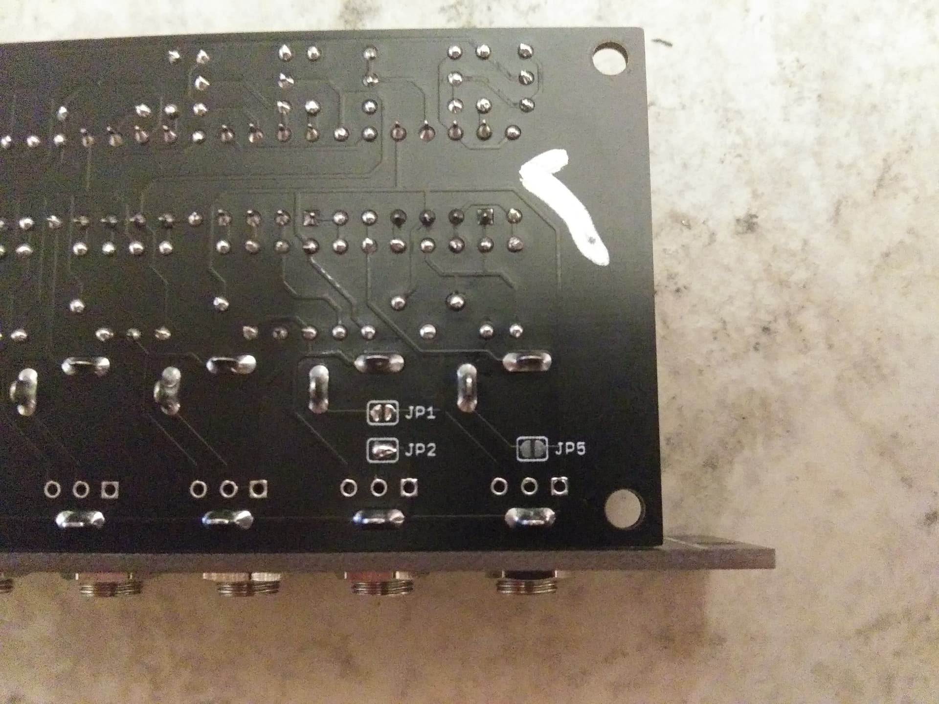
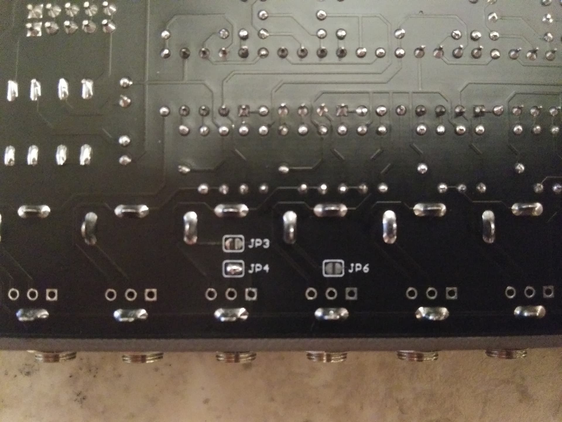
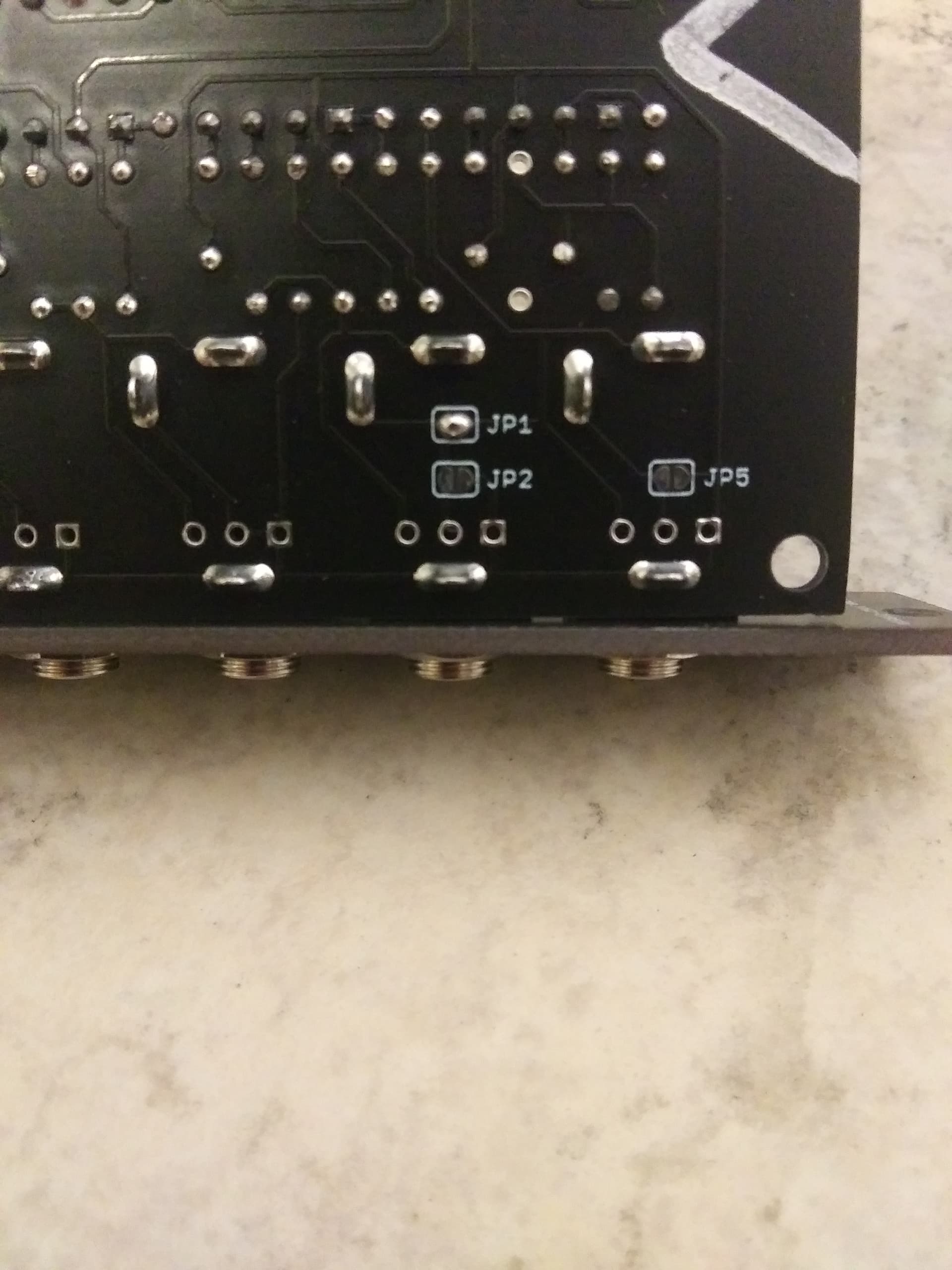
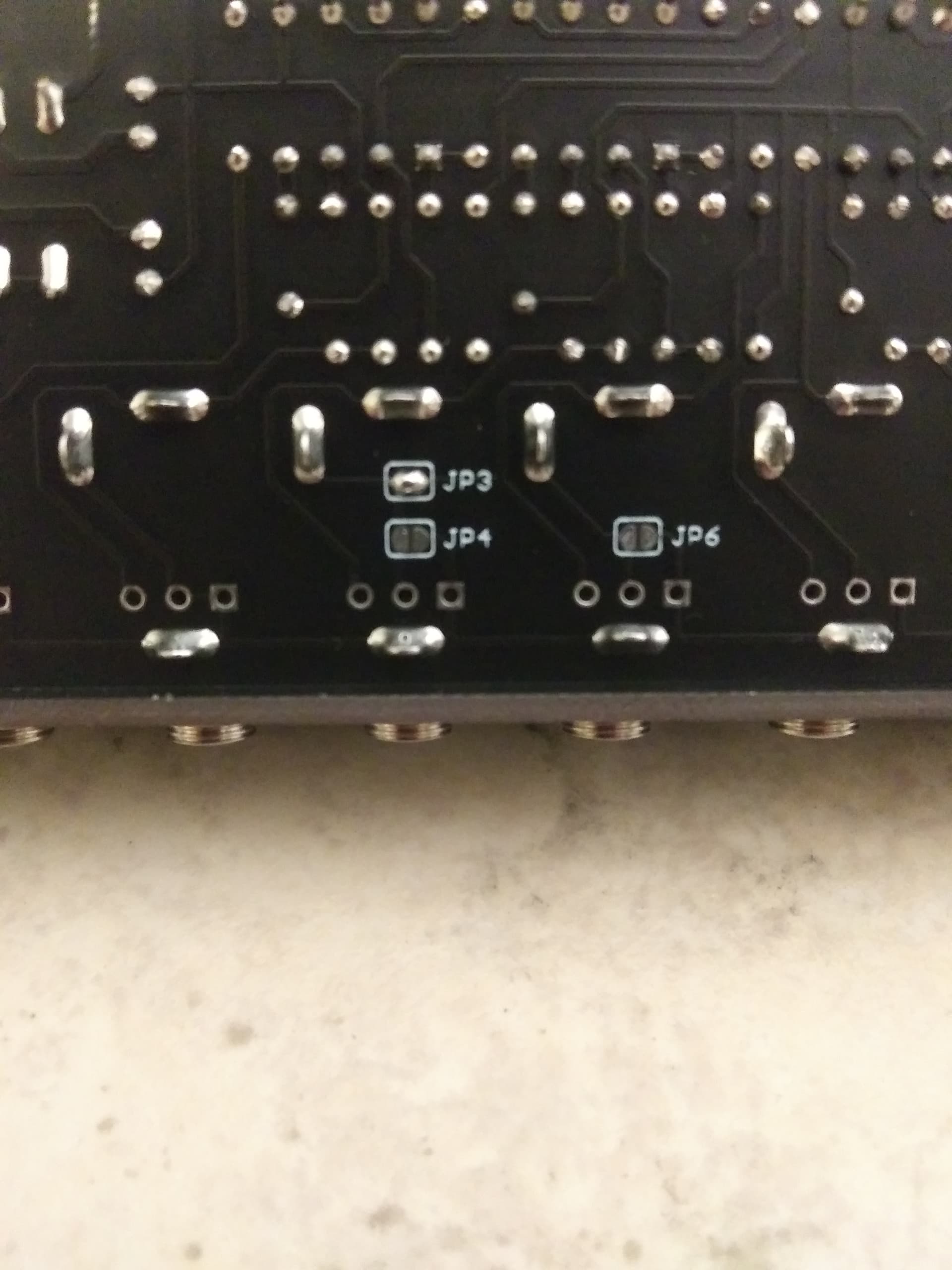
| 2 | Solder Jumpers | JP2, JP4 |
| 1 | PCB set | - |
| 1 | 10-16 Power ribbon | - |
| - | - | - |
| 5 | DNP | R38, JP1, JP3, JP5, JP6 |
*Solder jumpers are located on bottom-side of board.
*DNP means Do not populate.
*Unless specified differently, All resistors are always Metal Film type, 1/4W, 1% tolerance.
Build Guide for A+B-C
Step 0.
Using a PCB vice will improve your DIY experience immensely.
Step 1.
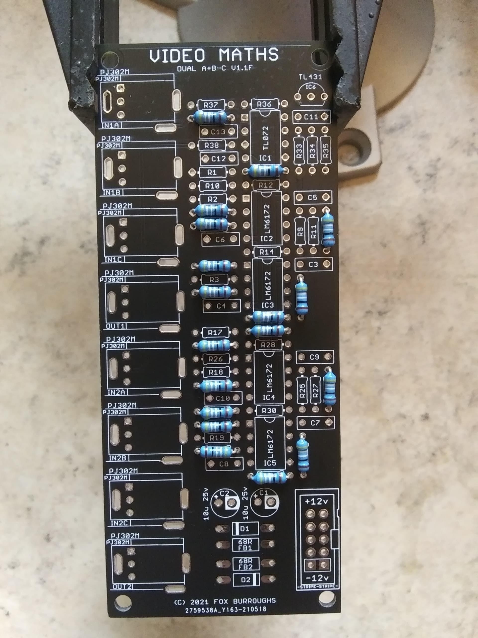
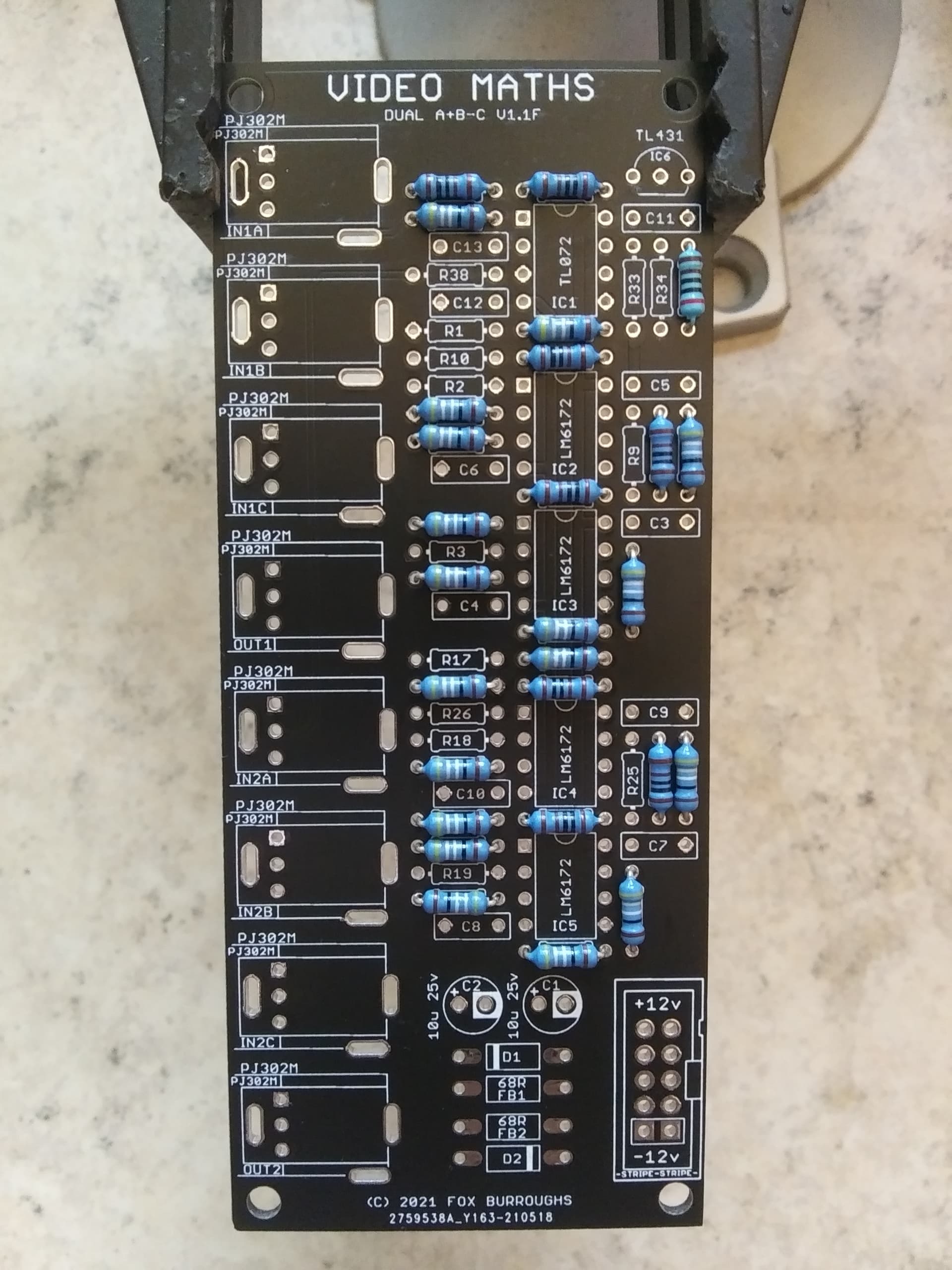
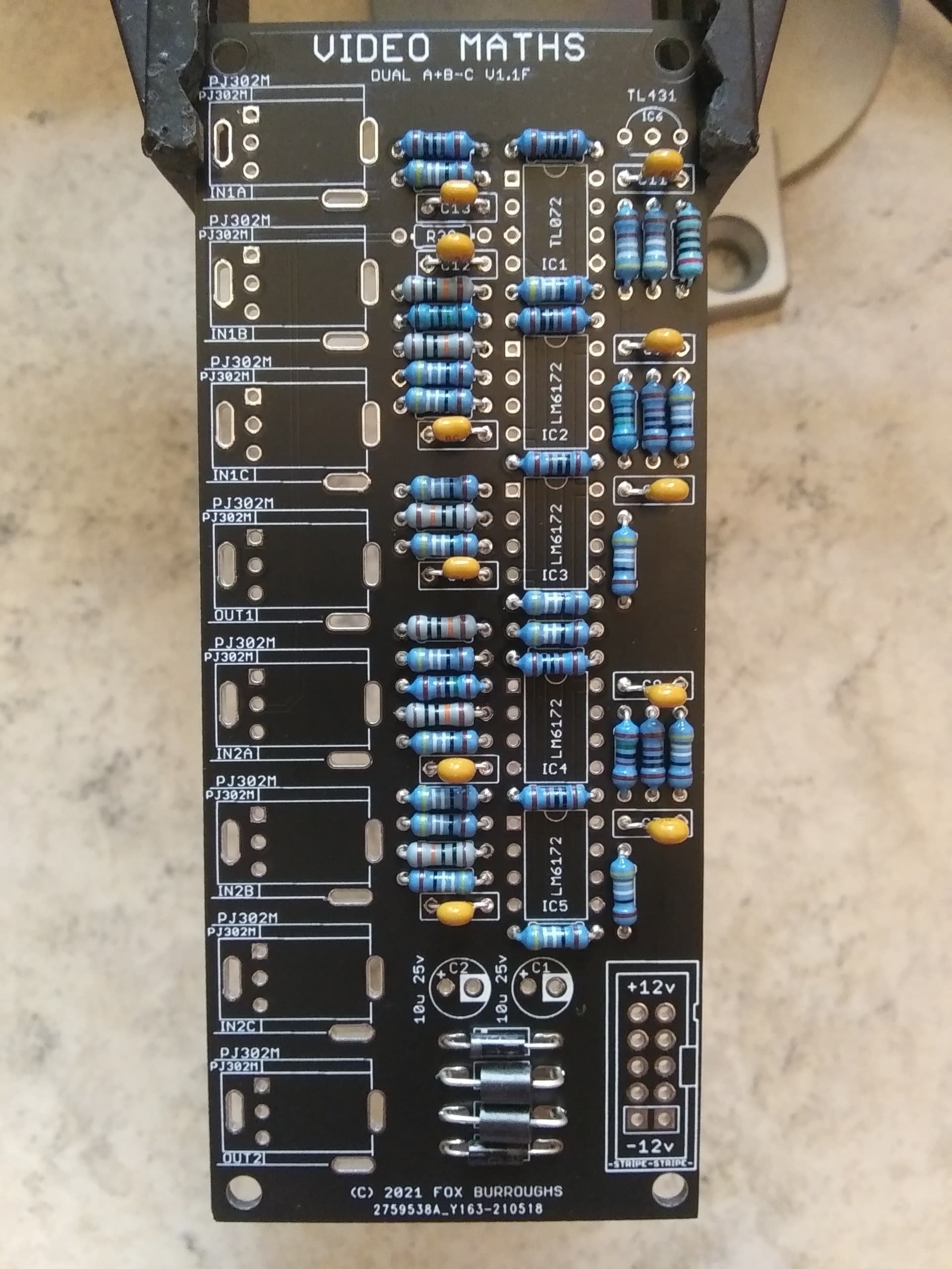
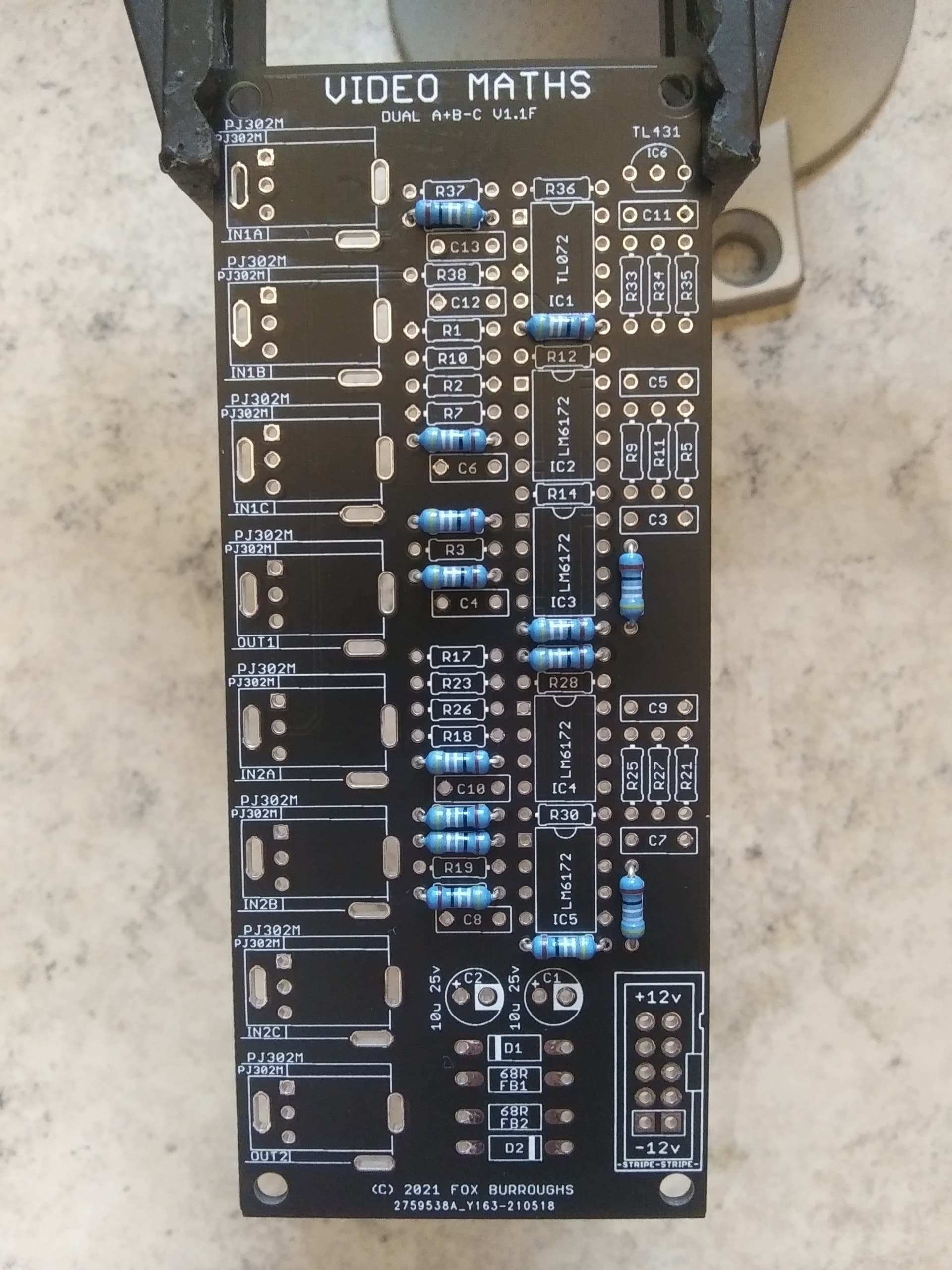
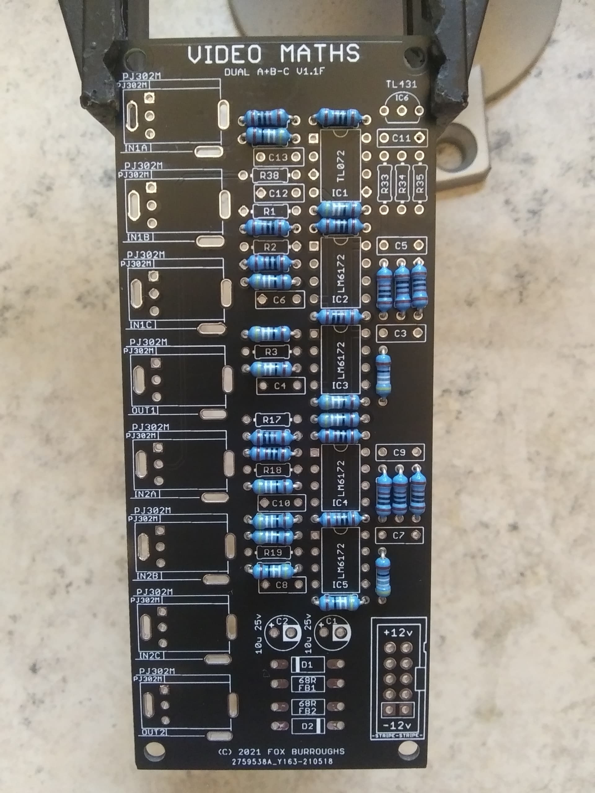
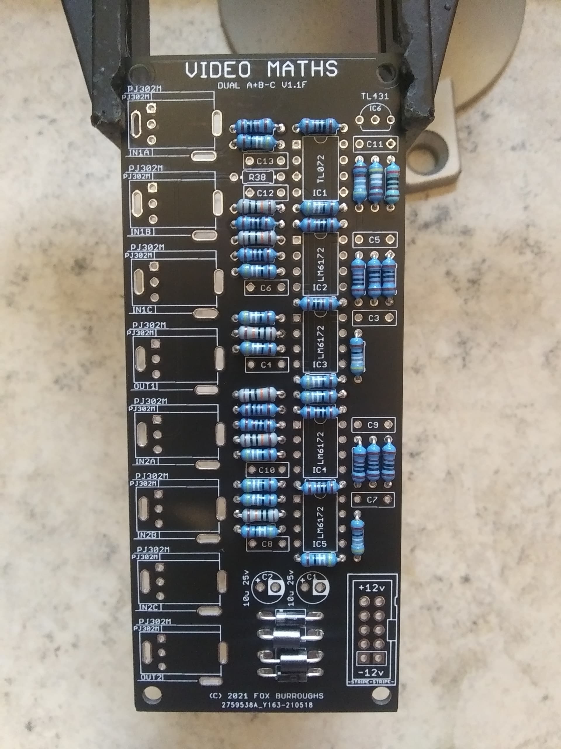
We will being with the 499R resistors. There are 18 of them: R4, R5, R6, R7, R8, R13, R15, R16, R20, R21, R22, R23, R24, R29, R31, R32, R39, R42.
Step 2.
Next are the 1K resistors: R11, R12, R14, R27, R28, R30, R36, R37
Step 3.
Just a single 2K resistor for this config, R35.
Step 4.
Next are two 4.99K resistors: R33, R34.
Step 5.
Six 100K resistors, R1, R2, R3, R17, R18, R19.
Step 6.
The last four resistors are 1.5K ohms: R9, R10, R25, R26.
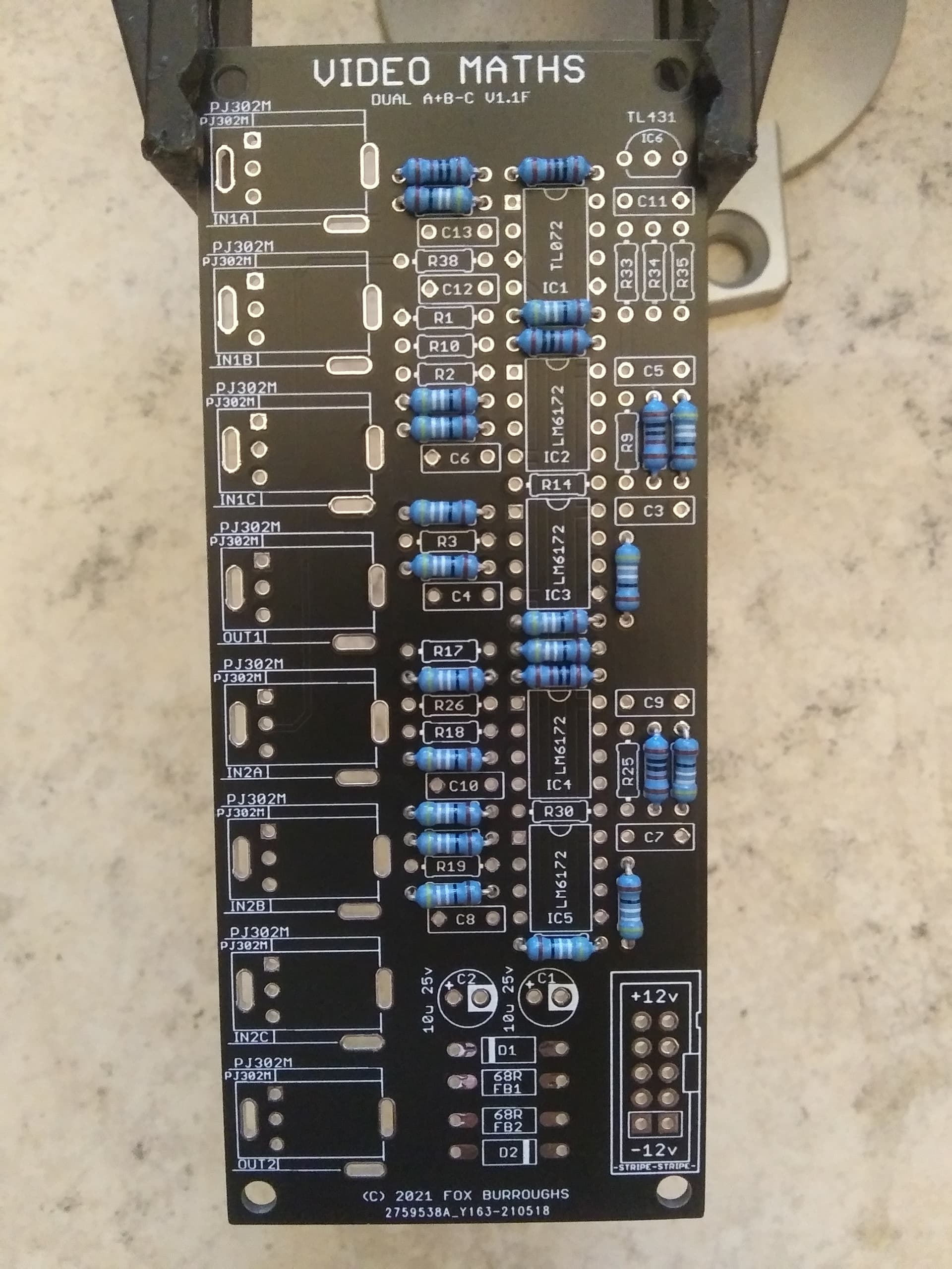
Step 7.
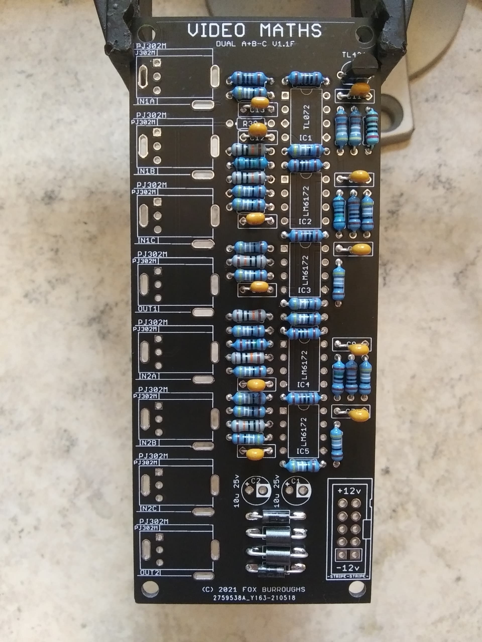
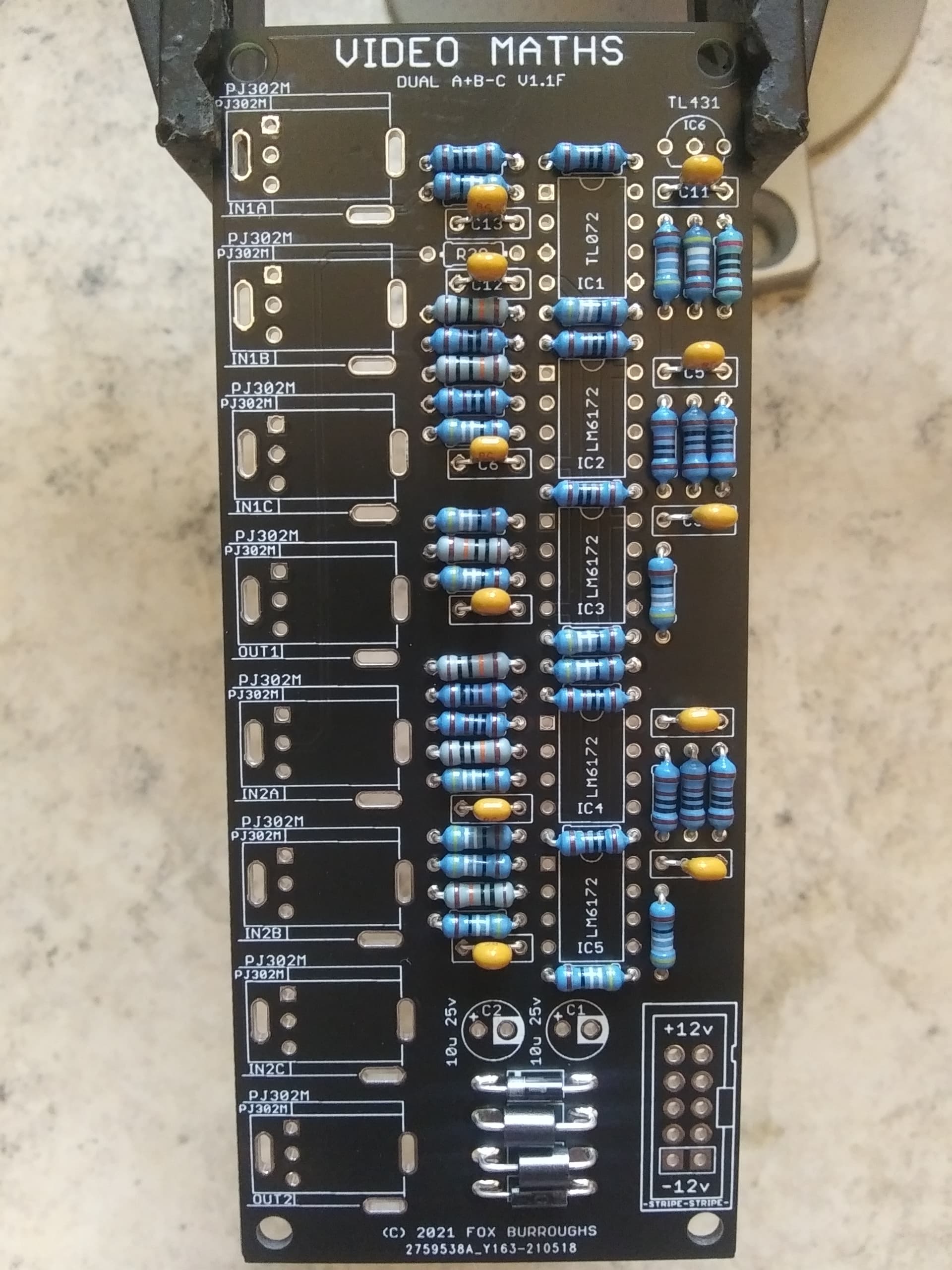
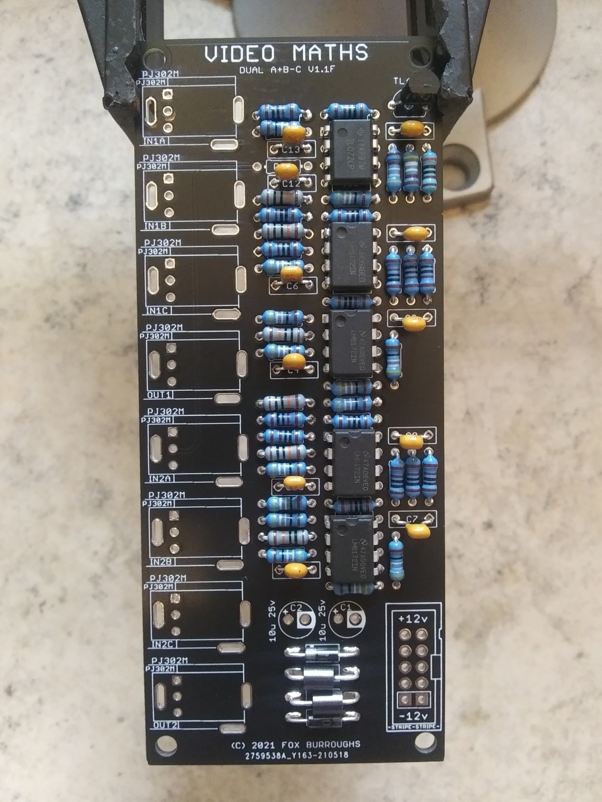
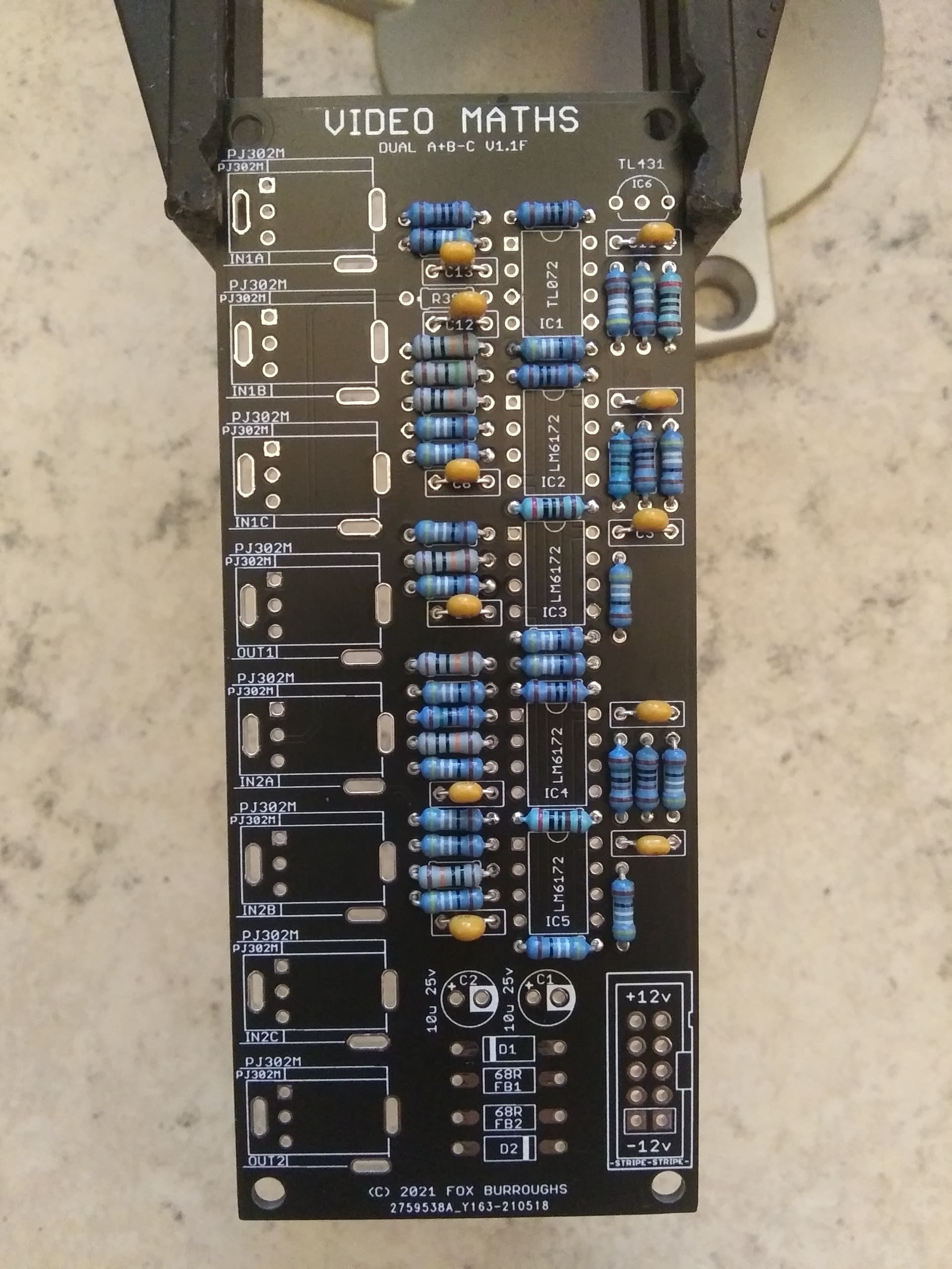
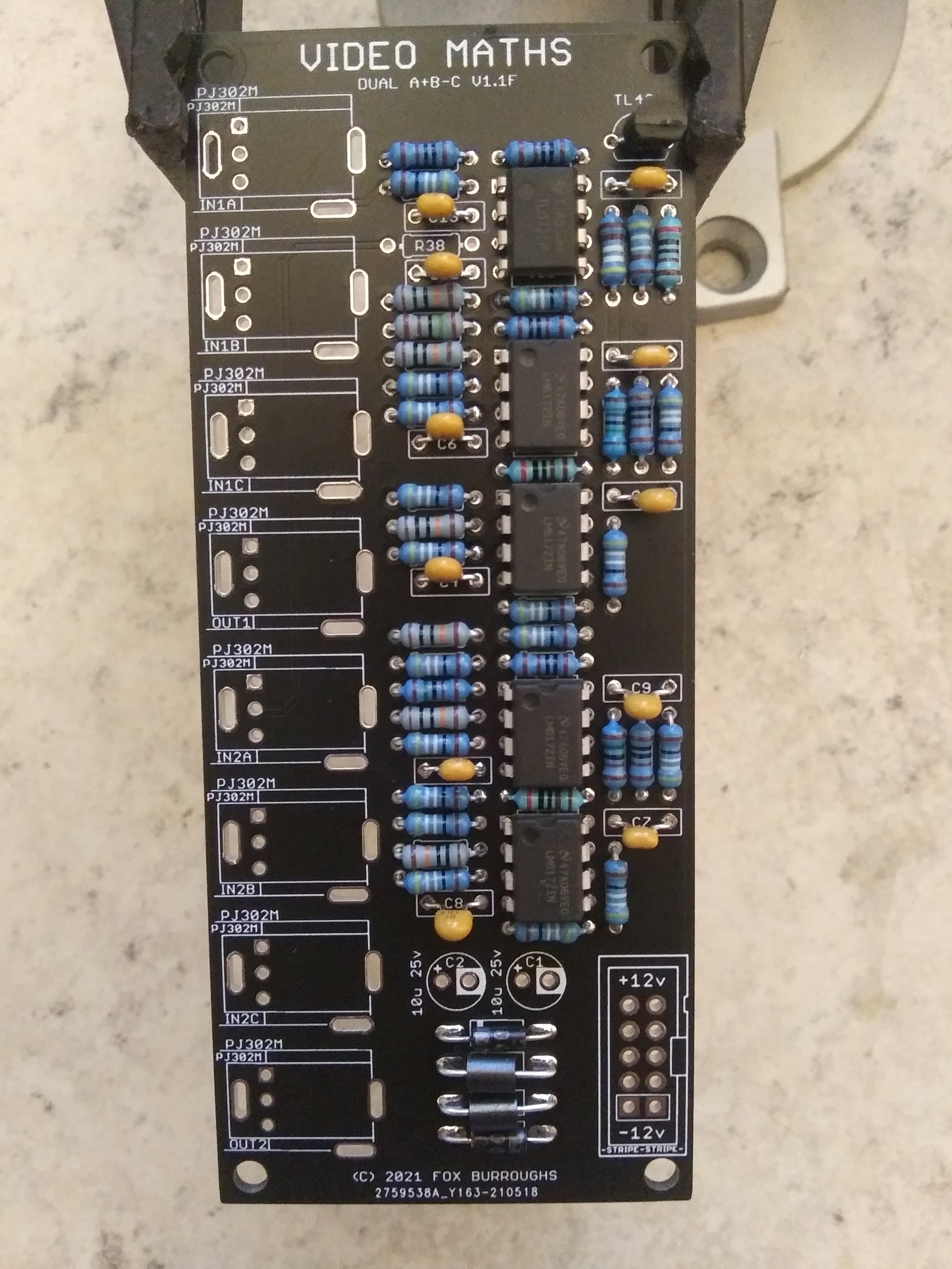
Here you can see that I’ve populated all eleven 100nF caps as well as both diodes and both ferrite beads. As always, make sure the stripes on the diodes line up with the stripes on the pcb.
Step 8.
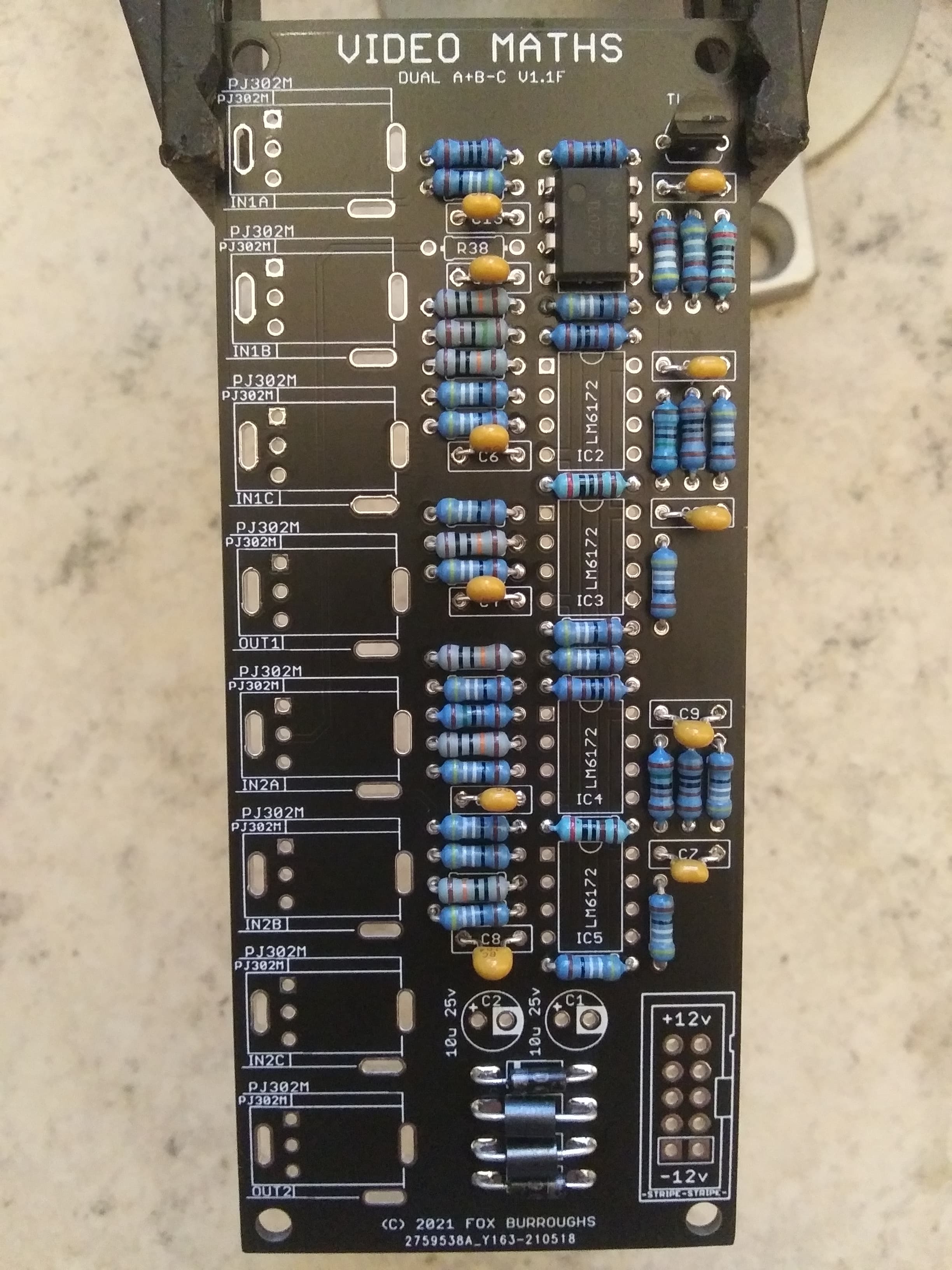
Next, add the TL431 voltage reference to the top right hand side of the pcb.
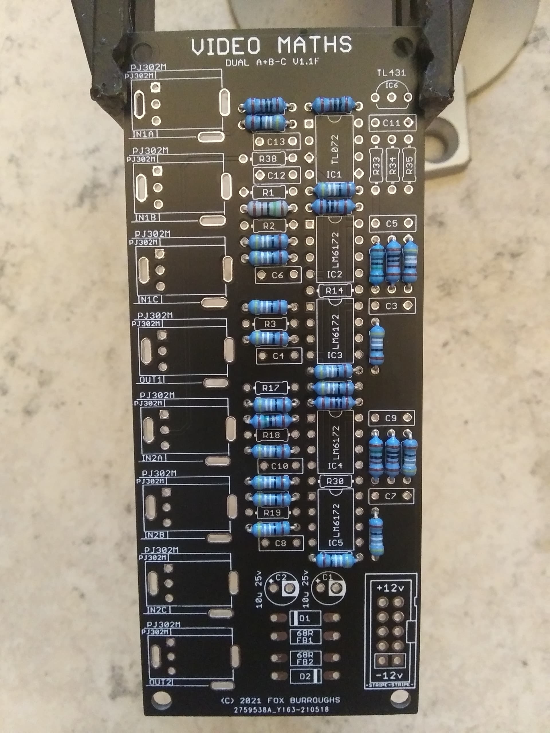
Step 9.
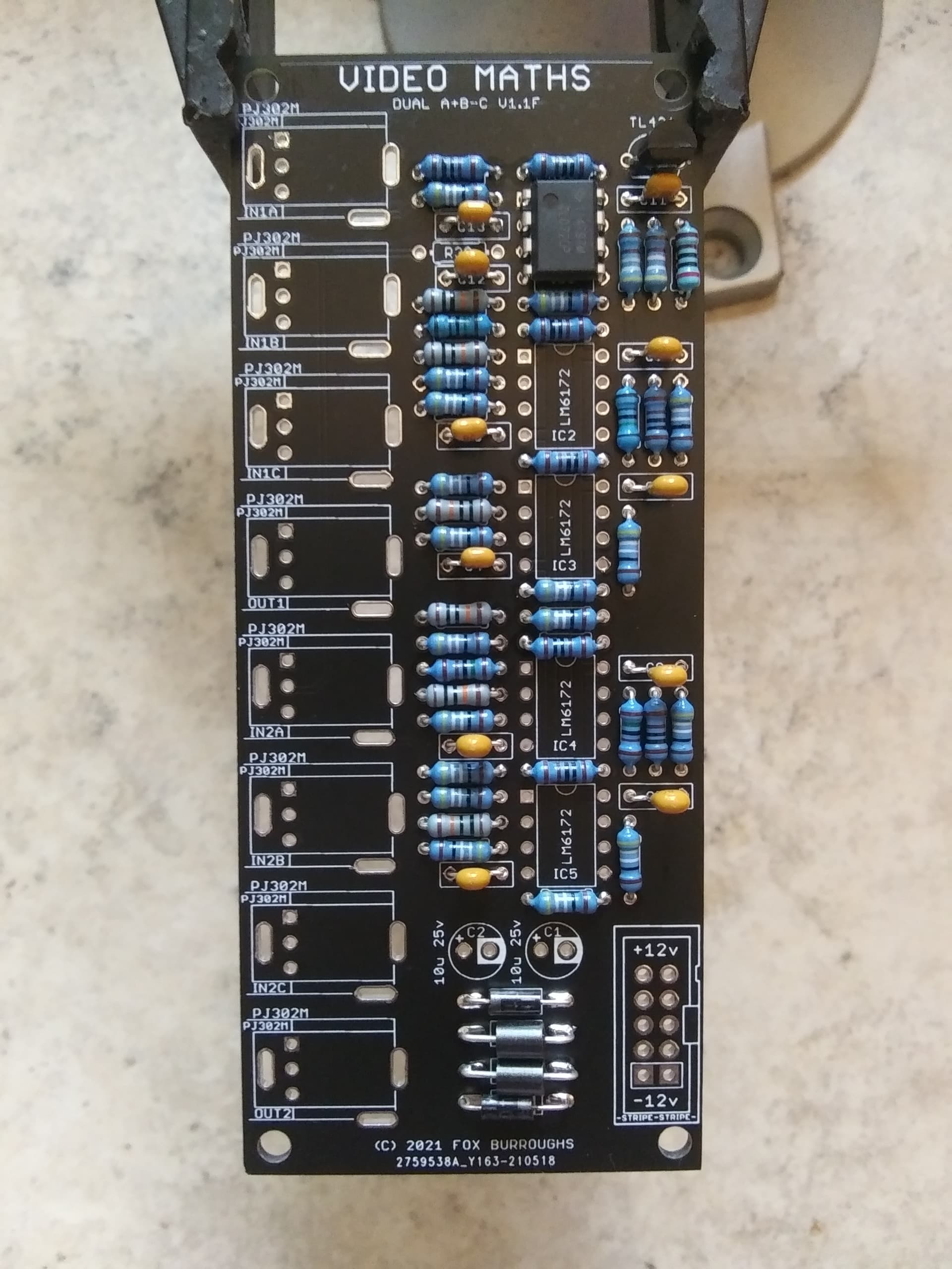
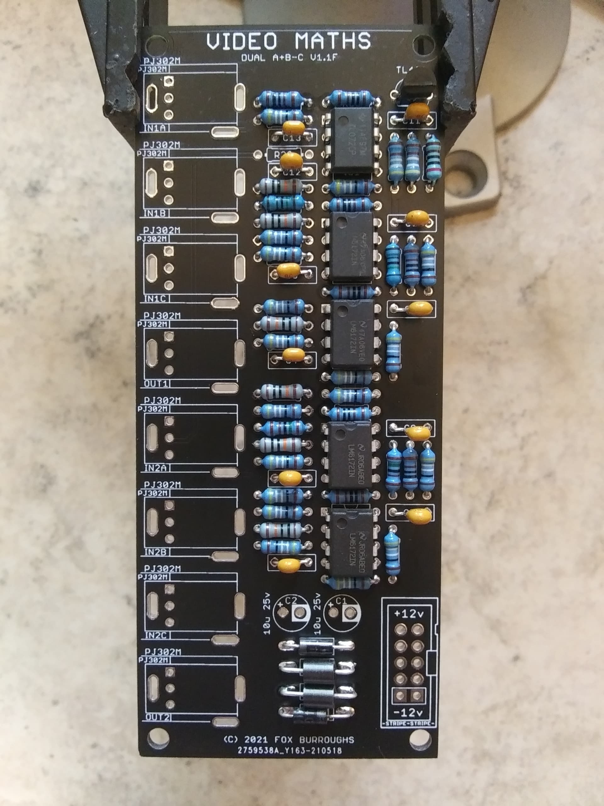
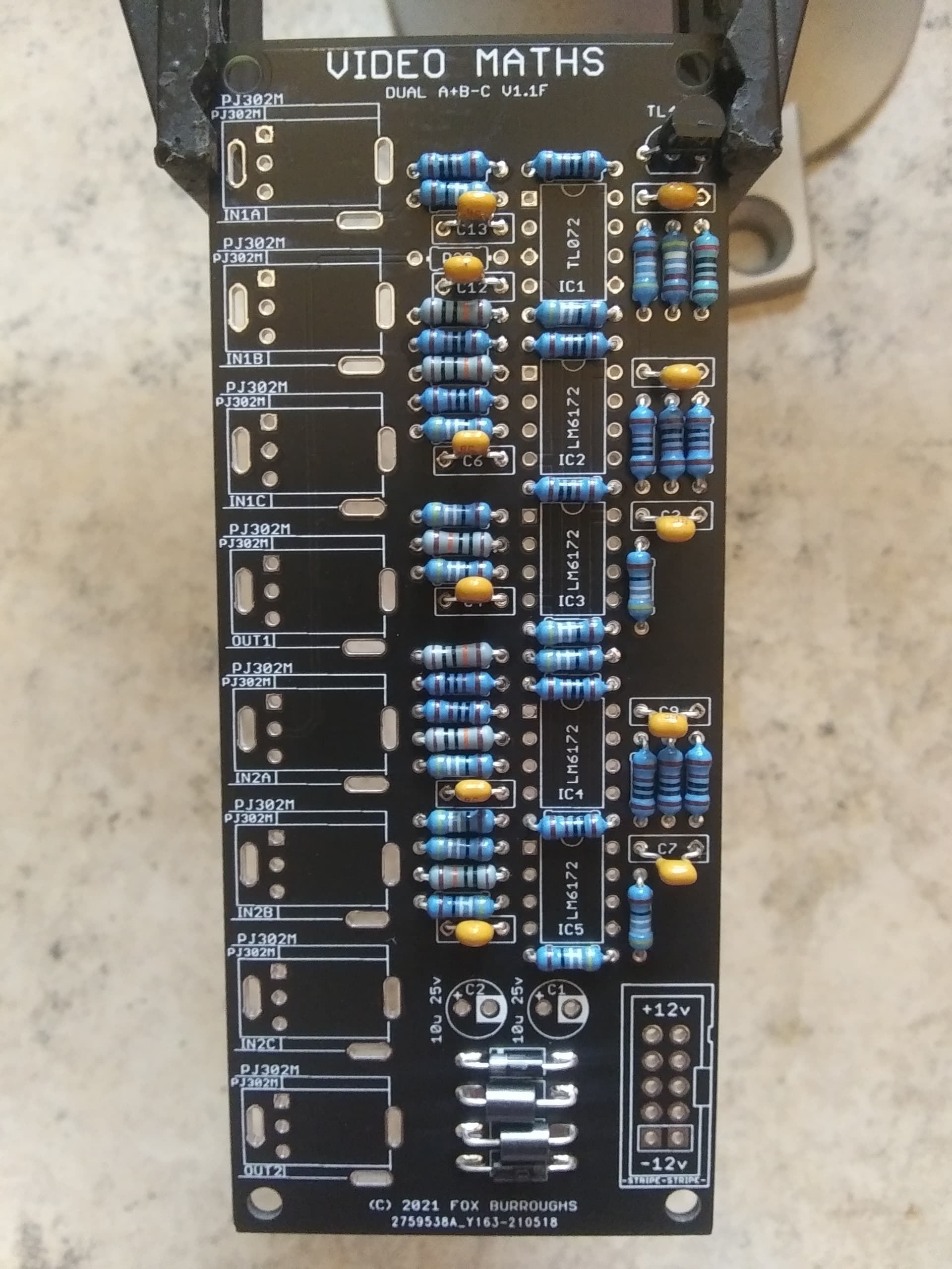
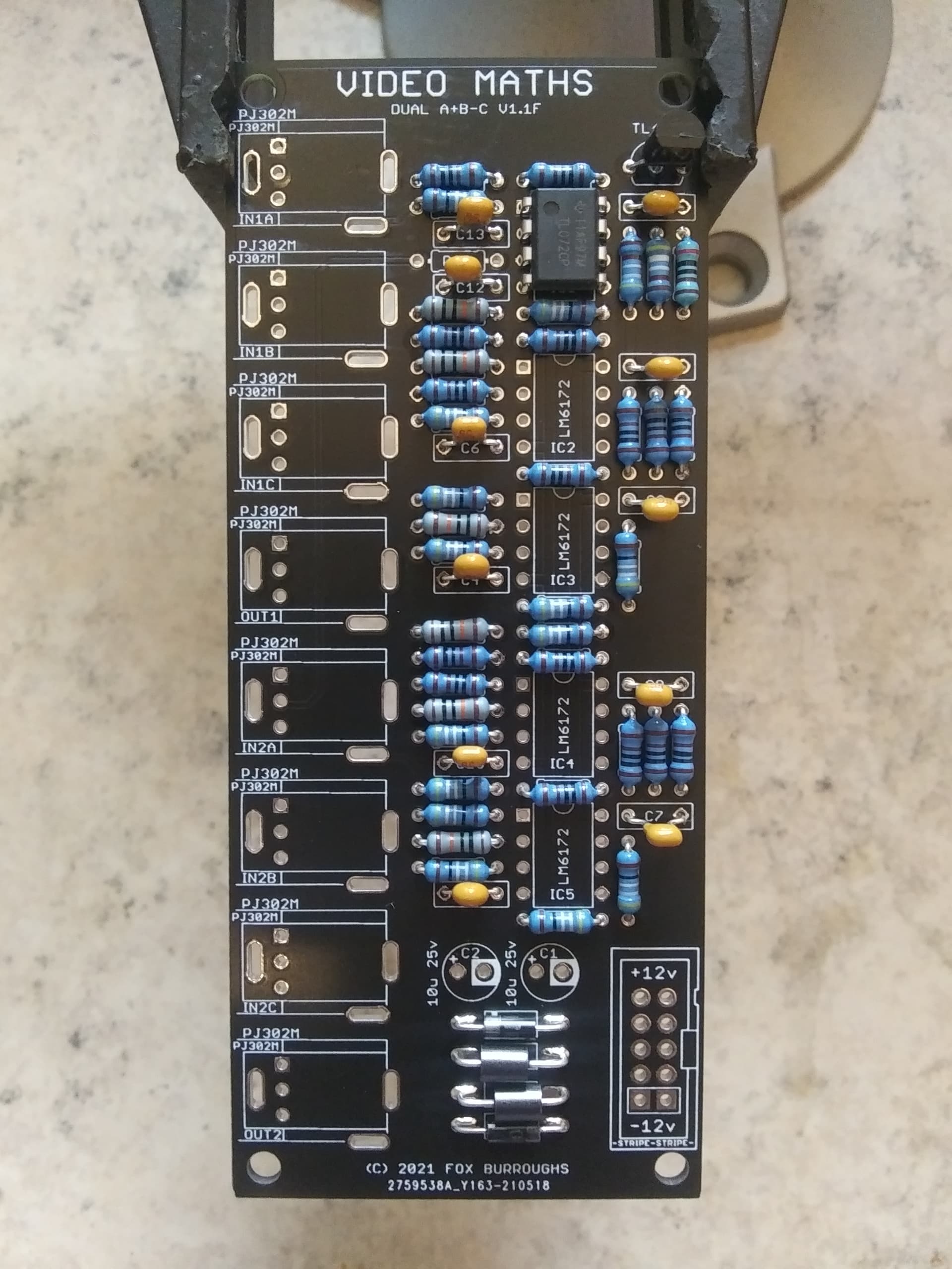
The top op amp is a TL072. Make sure pin 1 is lined up with the square via.
Step 10.
The four remaining op amps are LM6172’s. Again, make sure pin 1 of each IC is lined up with the square vias.
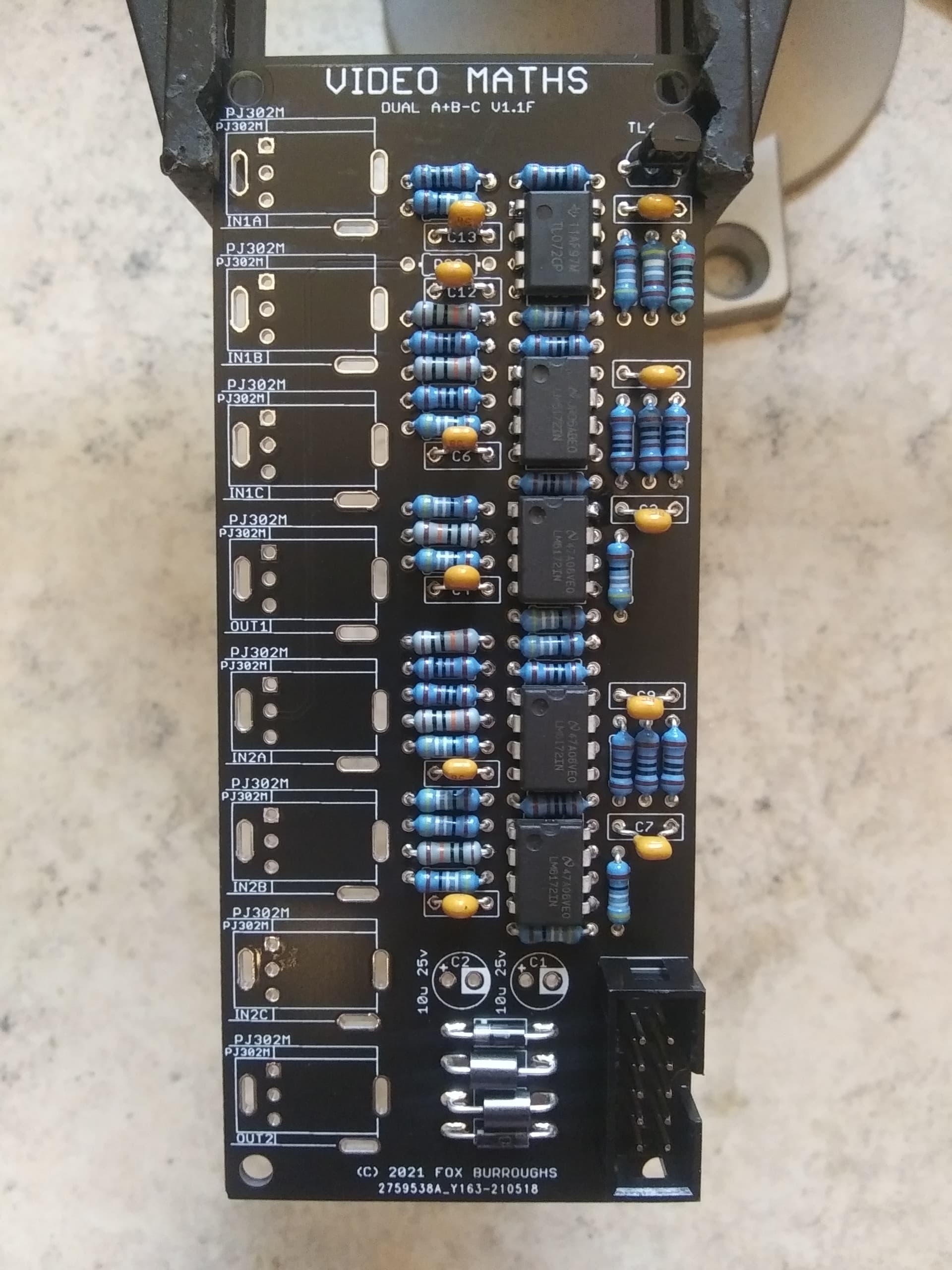
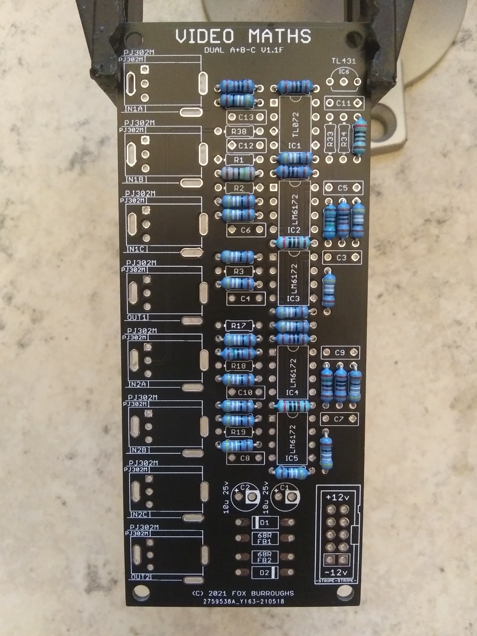
Step 11.
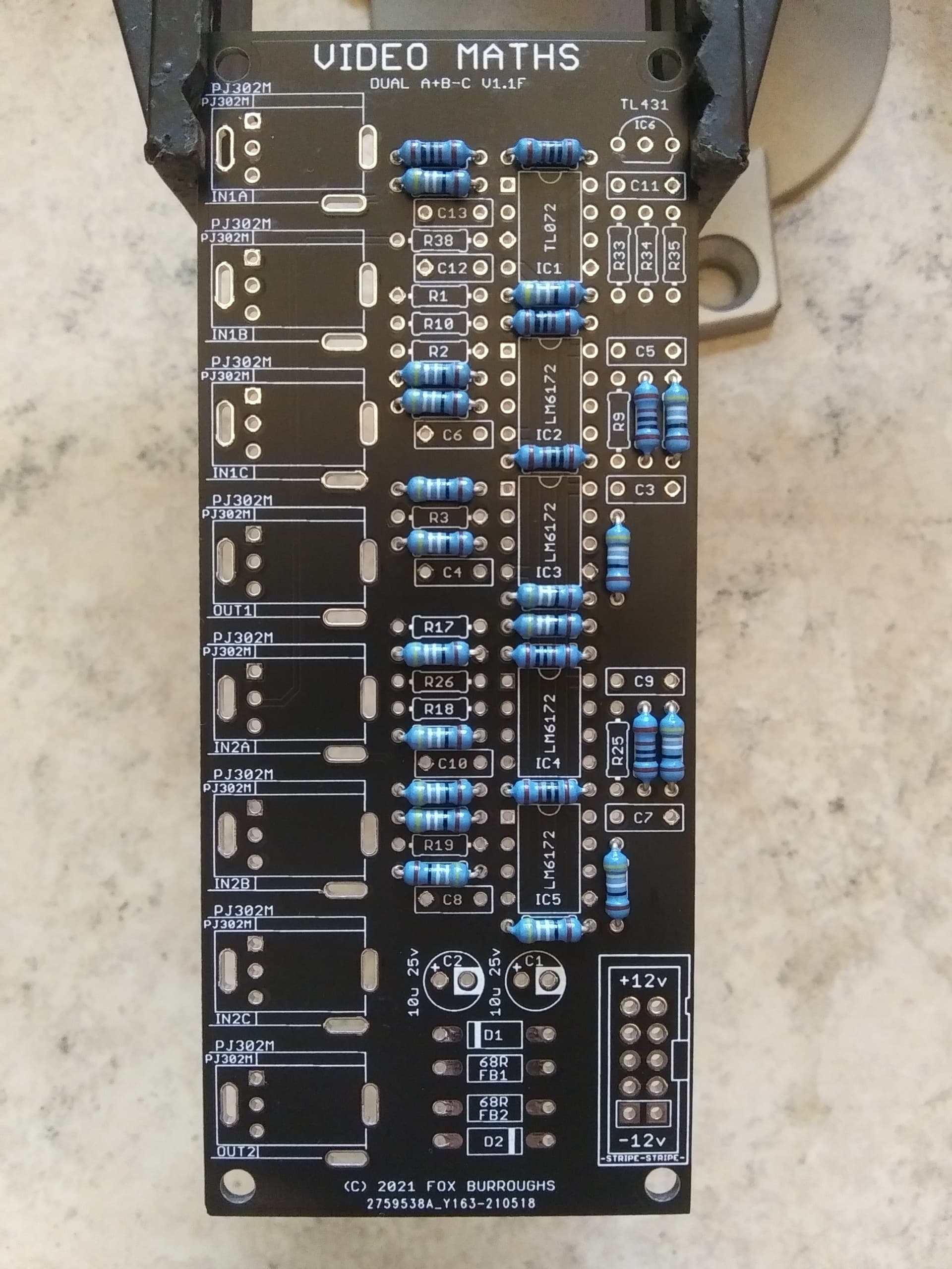
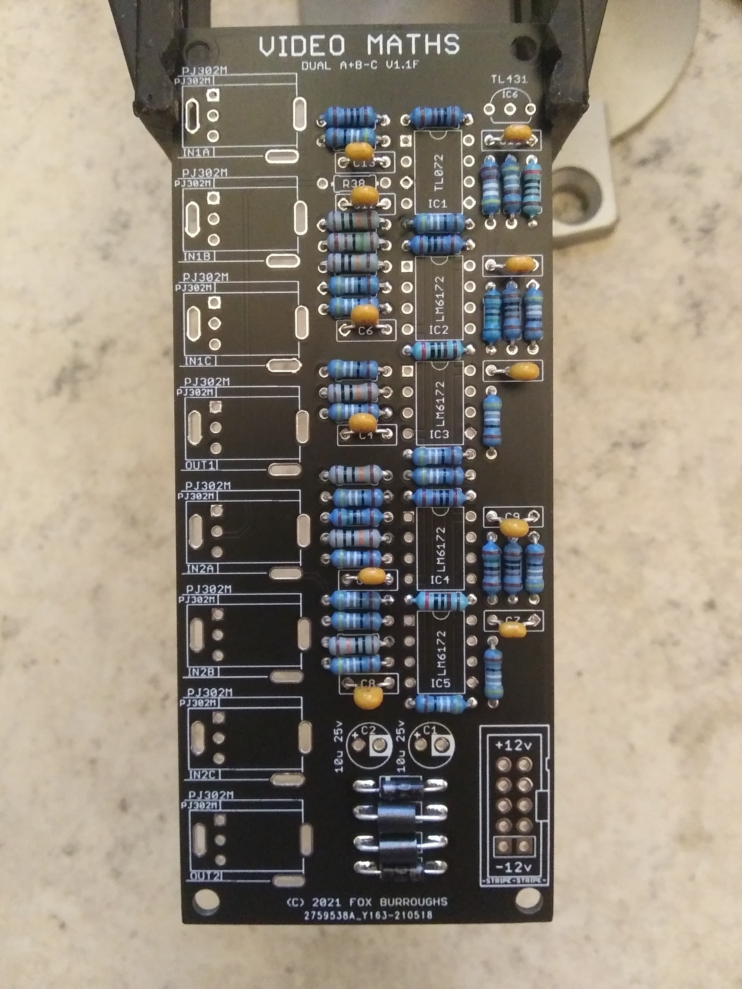
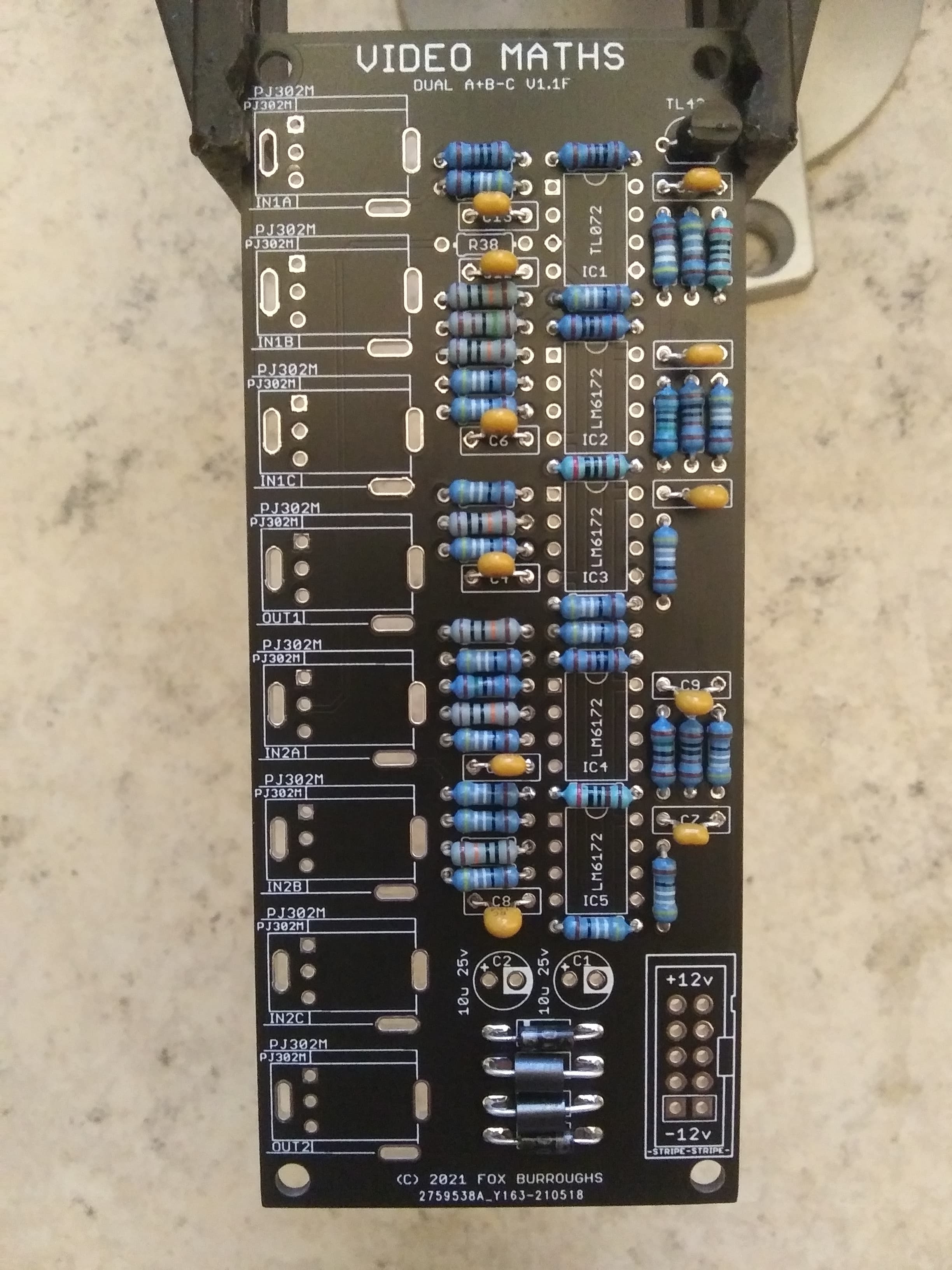
The next tallest component is the 10-pin shrouded power connector. The “notch” or “key” faces outward to the right.
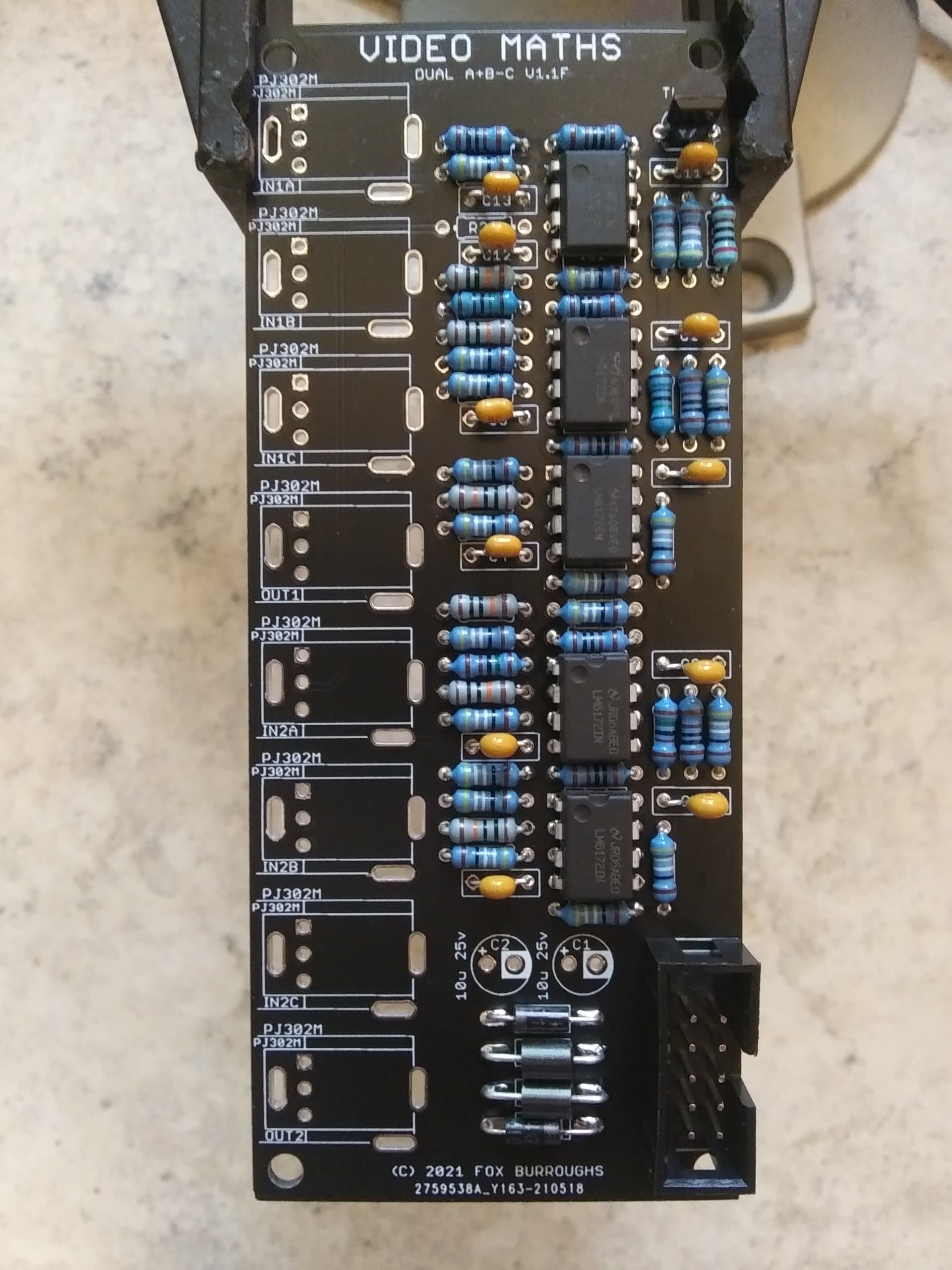
Step 12.
Now populate both electrolytic caps. These are polarized parts and the stripe down the side designates the negative lead. Place the negative lead into the via that is circled.
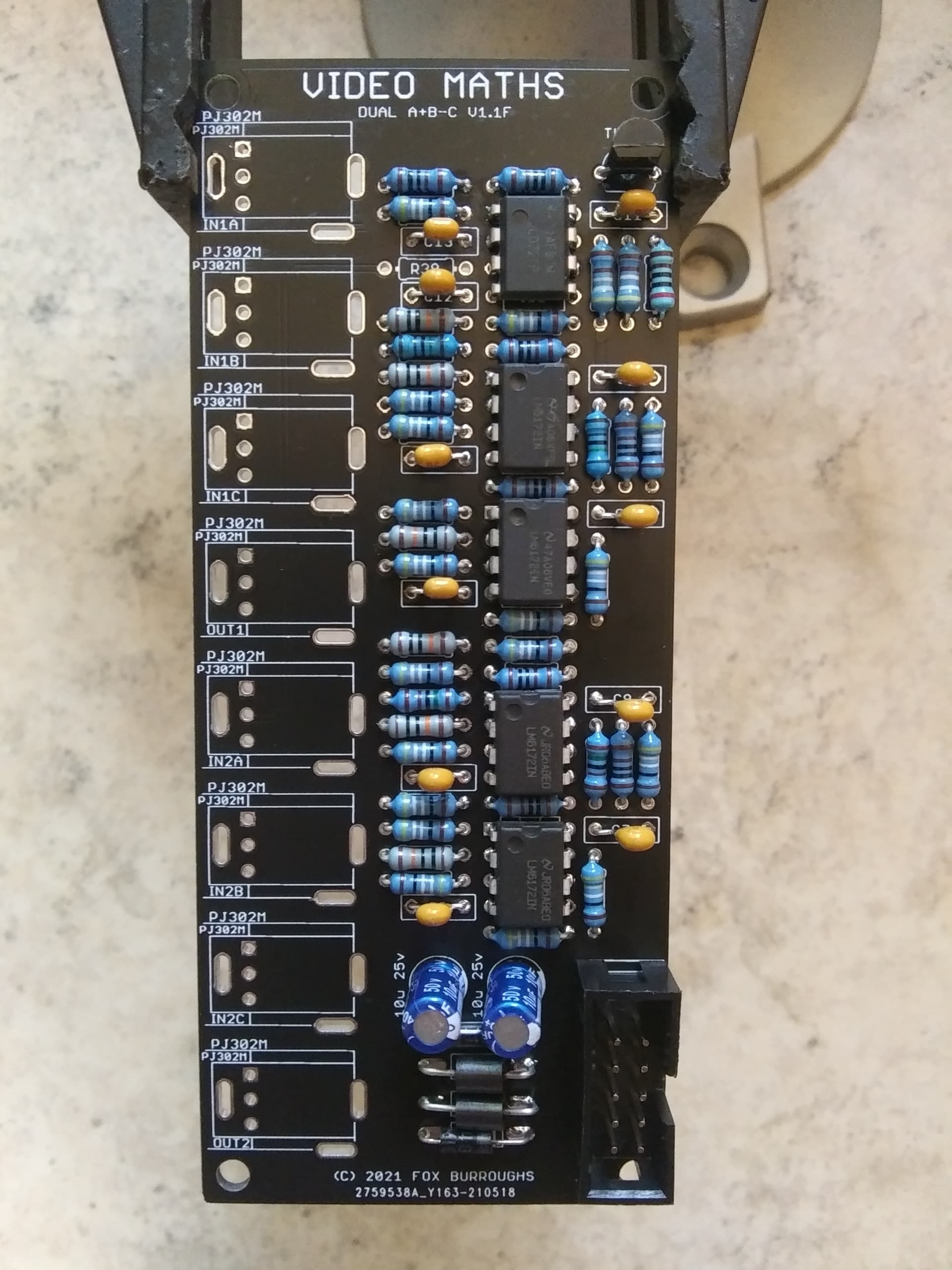
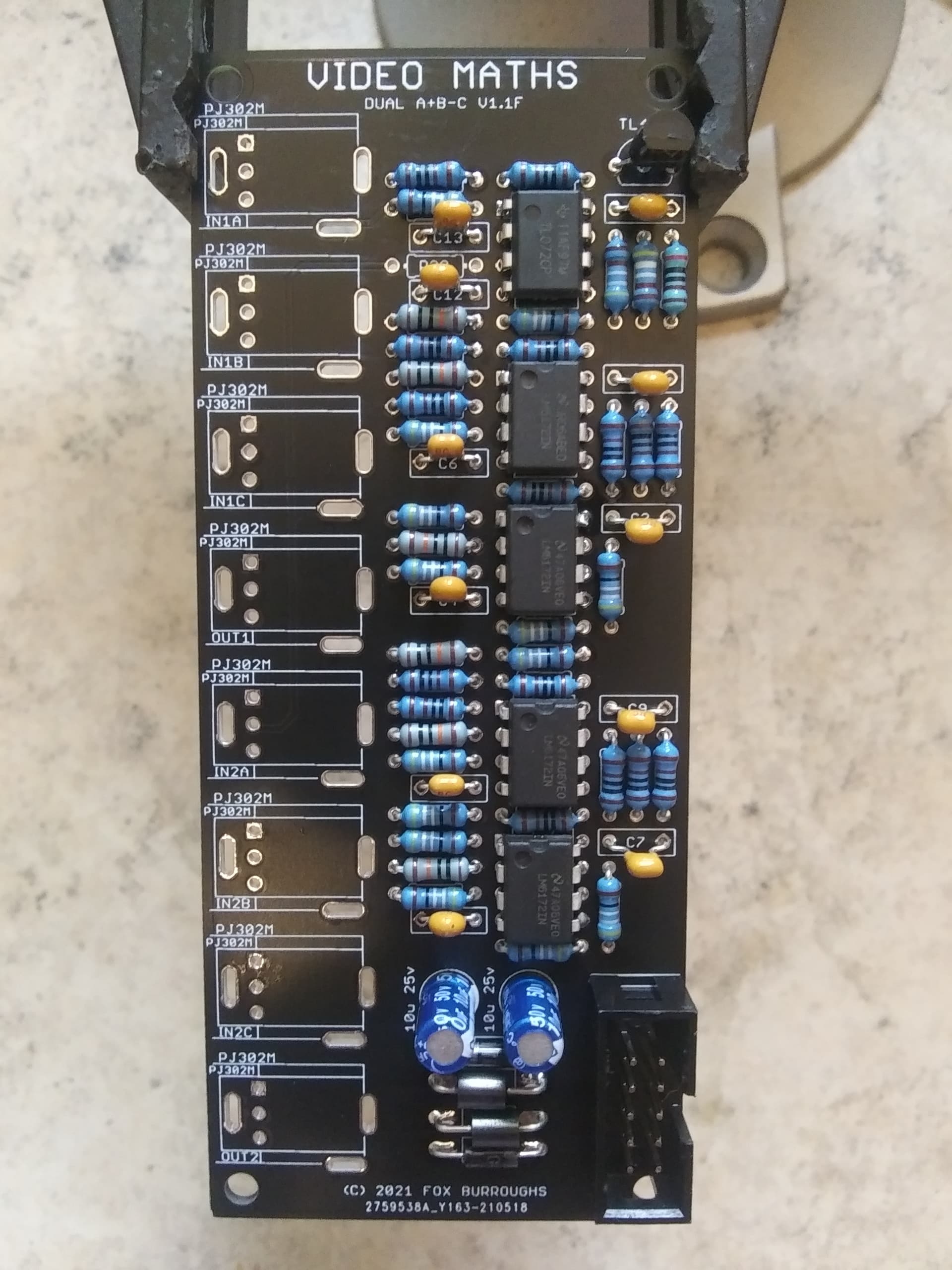
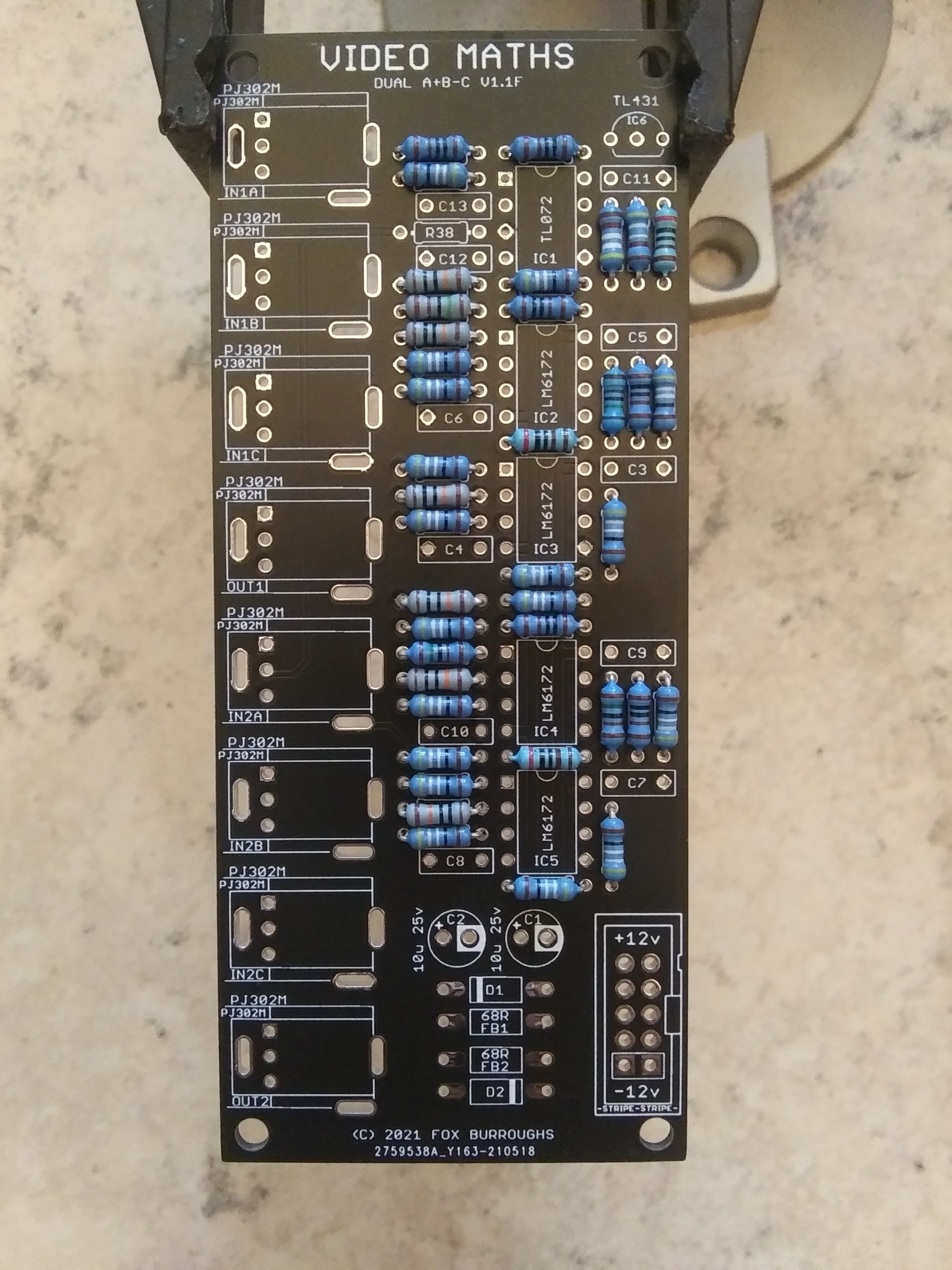
Step 13.
There are eight PJ302M jacks. Place each of them into the board and install the faceplate carefully. Finger-tighten a nut onto each jack and make sure they are lined up straight before soldering.
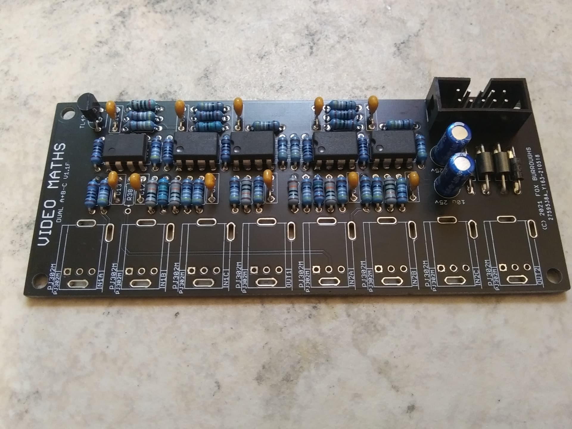
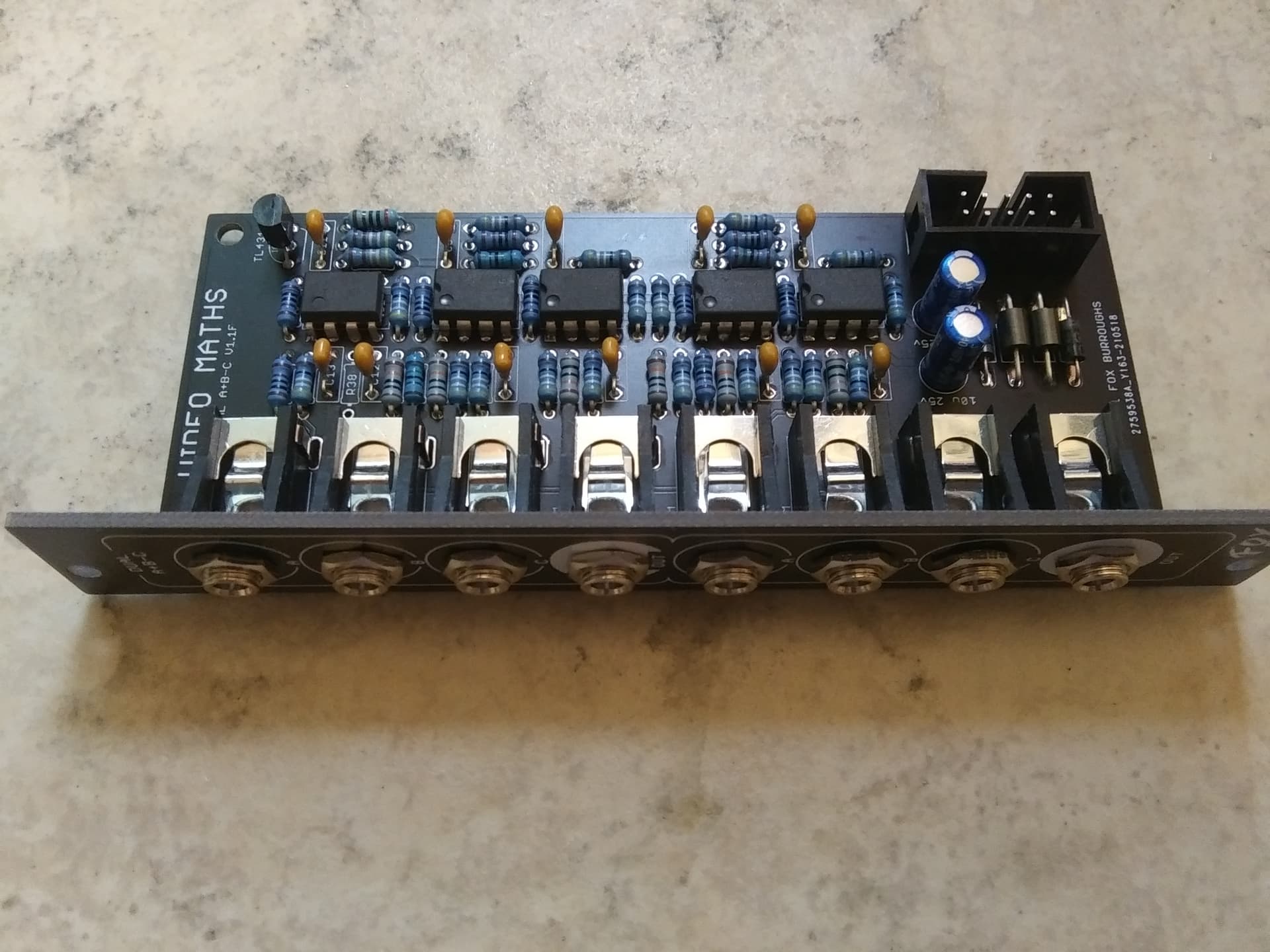
Step 14.
Finally, we will add the solder-jumpers to the bottom of the board. This configuration requires JP2 and JP4 to be soldered. Do not solder the others.
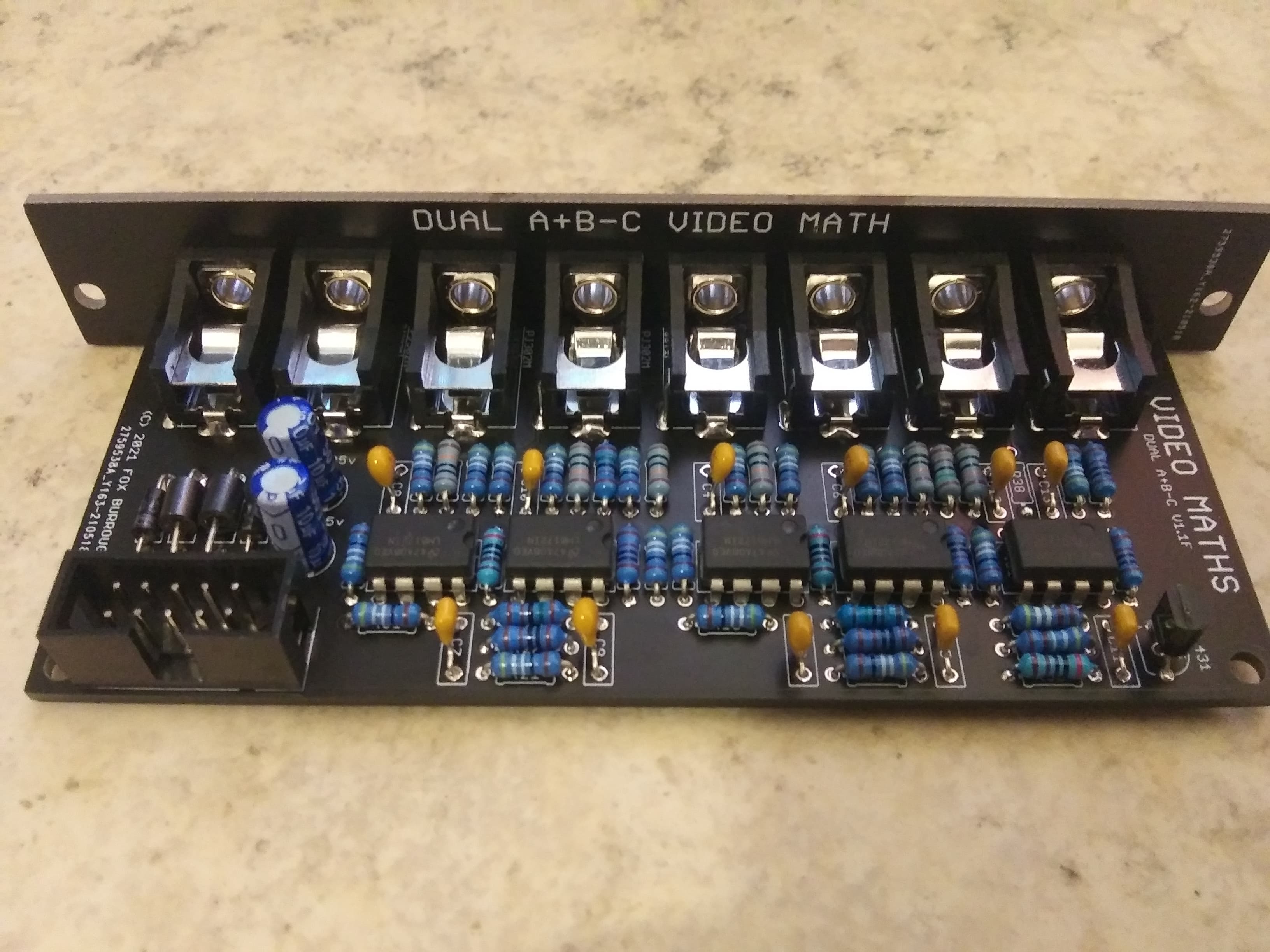
Clean up your board and test it out!
BOM for (A+B)/2-C configuration
| Qty | Value | Parts |
|---|---|---|
| 2 | 10u/25v capacitor | C1, C2 |
| 11 | 100n capacitor | C3, C4, C5, C6, C7, C8, C9, C10, C11, C12, C13 |
| 1 | 10-Pin Box Header | CONN9 |
| 2 | 1N4001 diode | D1, D2 |
| 2 | 68R ferrite bead | FB1, FB2 |
| 1 | TL072 IC | IC1 |
| 4 | LM6172 IC | IC2, IC3, IC4, IC5 |
| 1 | TL431 | IC6 |
| 8 | PJ302M jacks | IN1A, IN1B, IN1C, IN2A, IN2B, IN2C, OUT1, OUT2 |
| 14 | 499R resistor | R4, R6, R8, R13, R15, R16, R20, R22, R24, R29, R31, R32, R39, R42 |
| 16 | 1K resistor | R5, R7, R9, R10, R11, R12, R14, R21, R23, R25, R26, R27, R28, R30, R36, R37 |
| 1 | 2K resistor | R35 |
| 2 | 4.99K resistor | R33, R34 |
| 6 | 100K resistor | R1, R2, R3, R17, R18, R19 |
| 2 | Solder Jumper | JP1, JP3 |
| 1 | PCB set | - |
| 1 | 10-16 Power ribbon | - |
| - | - | - |
| 5 | DNP | R38, JP2, JP4, JP5, JP6 |
*Solder jumpers are located on bottom-side of board.
*DNP means Do not populate.
*Unless specified differently, All resistors are always Metal Film type, 1/4W, 1% tolerance.
Build Guide for (A+B)/2-C
Step 0.
Using a PCB vice will improve your DIY experience immensely.
Step 1.
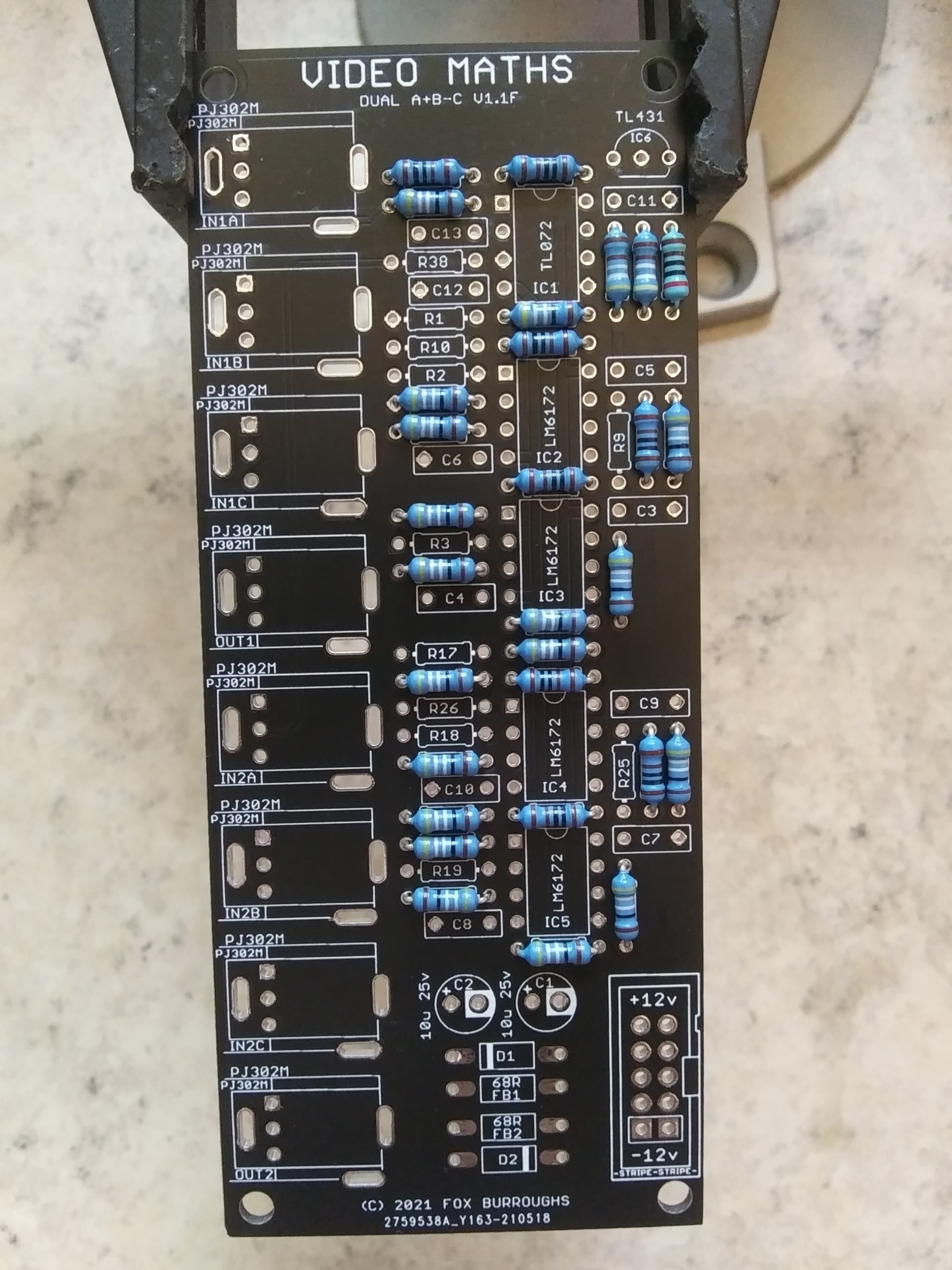
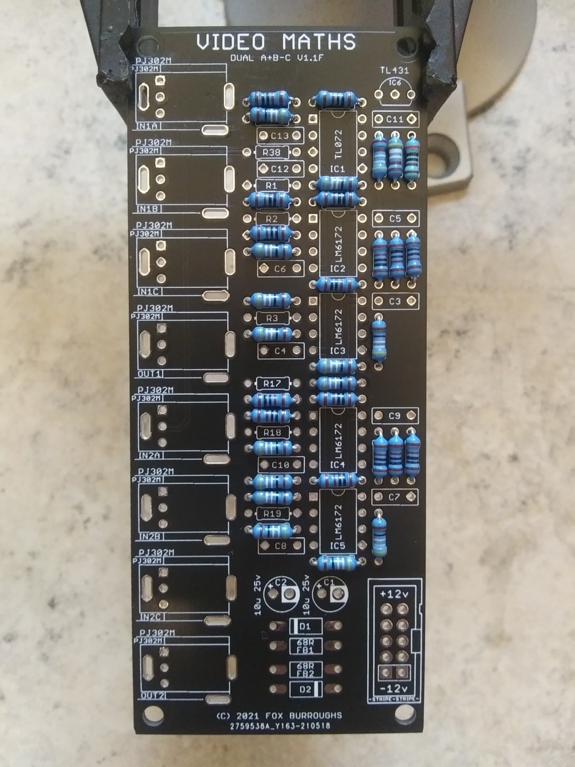
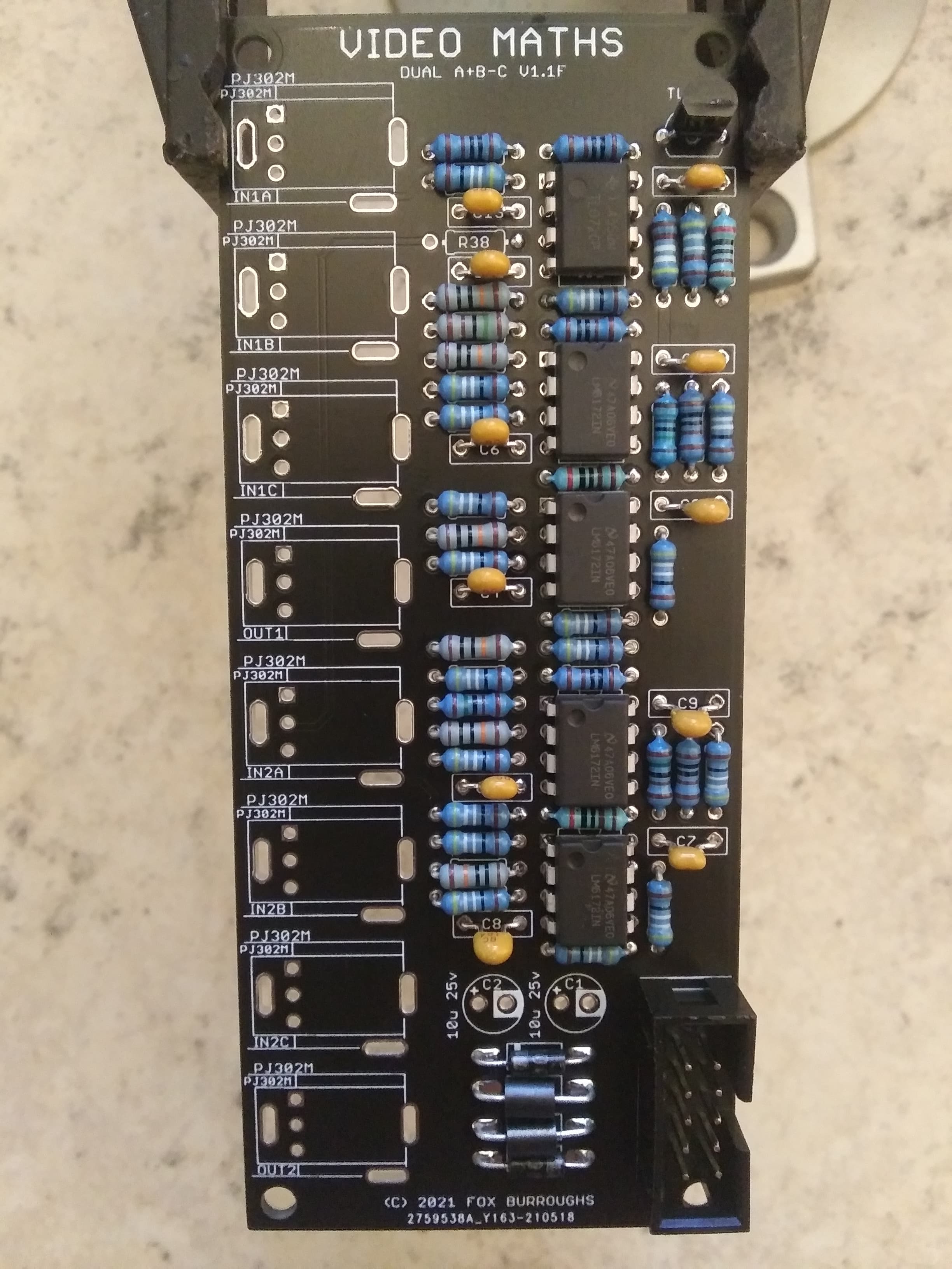
First, populate the 499R resistors. There are fourteen of them: R4, R6, R8, R13, R15, R16, R20, R22, R24, R29, R31, R32, R39, R42
Step 2.
Next populate all sixteen 1K resistors: R5, R7, R9, R10, R11, R12, R14, R21, R23, R25, R26, R27, R28, R30, R36, R37
Step 3.
There is only one 2K resistor needed: R35
Step 4.
Beside the resistor above, there are two 4.99K resistors: R33 and R34.
Step 5.
Finally, there are six 100K resistors: R1, R2, R3, R17, R18, R19. I prefer to solder all of the resistors at once.
Step 6.
Now populate both diodes and ferrite beads taking note of the diode’s polarity.
Step 7.
There are eleven 100nF caps to solder: C3, C4, C5, C6, C7, C8, C9, C10, C11, C12, C13
Step 8.
Now you may move on to the ICs. Start by soldering the TL431 in place, IC6. The first 8-pin op amp is a TL072, IC1. And finally you may solder IC2-IC5, all if which are LM6172. Make sure pin one for each of these is lined up correctly.
Step 9.
Then you may populate the 10-pin power header and both electrolytic caps. The power connector has a notch which needs to be lined up as shown on the silk screen.
Take special note of the polarity of the caps as well. Line up the stripe on each cap (negative) with the circled vias on the silkscreen.
Step 10.
There are eight PJ302M jacks. Place each of them into the board and install the faceplate carefully. Finger-tighten a nut onto each jack and make sure they are lined up straight before soldering.
Step 11.
Finally the last step is to add solder blobs to the jumpers on the bottom of the board. For this configuration, solder JP1 and JP3.
Thats it. Clean up your board and test!
BOM for (A+B-C)/2 configuration
| Qty | Value | Parts |
|---|---|---|
| 1 | 10-Pin Box Header | CONN9 |
| 11 | 100n | C3, C4, C5, C6, C7, C8, C9, C10, C11, C12, C13 |
| 2 | 10u 25v | C1, C2 |
| 18 | 499R | R4, R5, R6, R7, R8, R13, R15, R16, R20, R21, R22, R23, R24, R29, R31, R32, R39, R42 |
| 6 | 1K | R11, R12, R27, R28, R36, R37 |
| 4 | 1.5K | R9, R10, R25, R26 |
| 3 | 2K | R14, R30, R35 |
| 2 | 4.99K | R33, R34 |
| 6 | 100K | R1, R2, R3, R17, R18, R19 |
| 2 | 1N4001 | D1, D2 |
| 2 | 68R | FB1, FB2 |
| 4 | LM6172 | IC2, IC3, IC4, IC5 |
| 8 | PJ302M | IN1A, IN1B, IN1C, IN2A, IN2B, IN2C, OUT1, OUT2 |
| 1 | TL072 | IC1 |
| 1 | TL431 | IC6 |
| 2 | Solder Jumper | JP1, JP3 |
| - | - | - |
| 5 | DNP | JP2, JP4, JP5, JP6, R38 |
*Solder jumpers are located on bottom-side of board.
*DNP means Do not populate.
*Unless specified differently, All resistors are always Metal Film type, 1/4W, 1% tolerance.
Build Guide for (A+B-C)/2
Step 0.
Using a PCB vice will improve your DIY experience immensely.
Step 1.
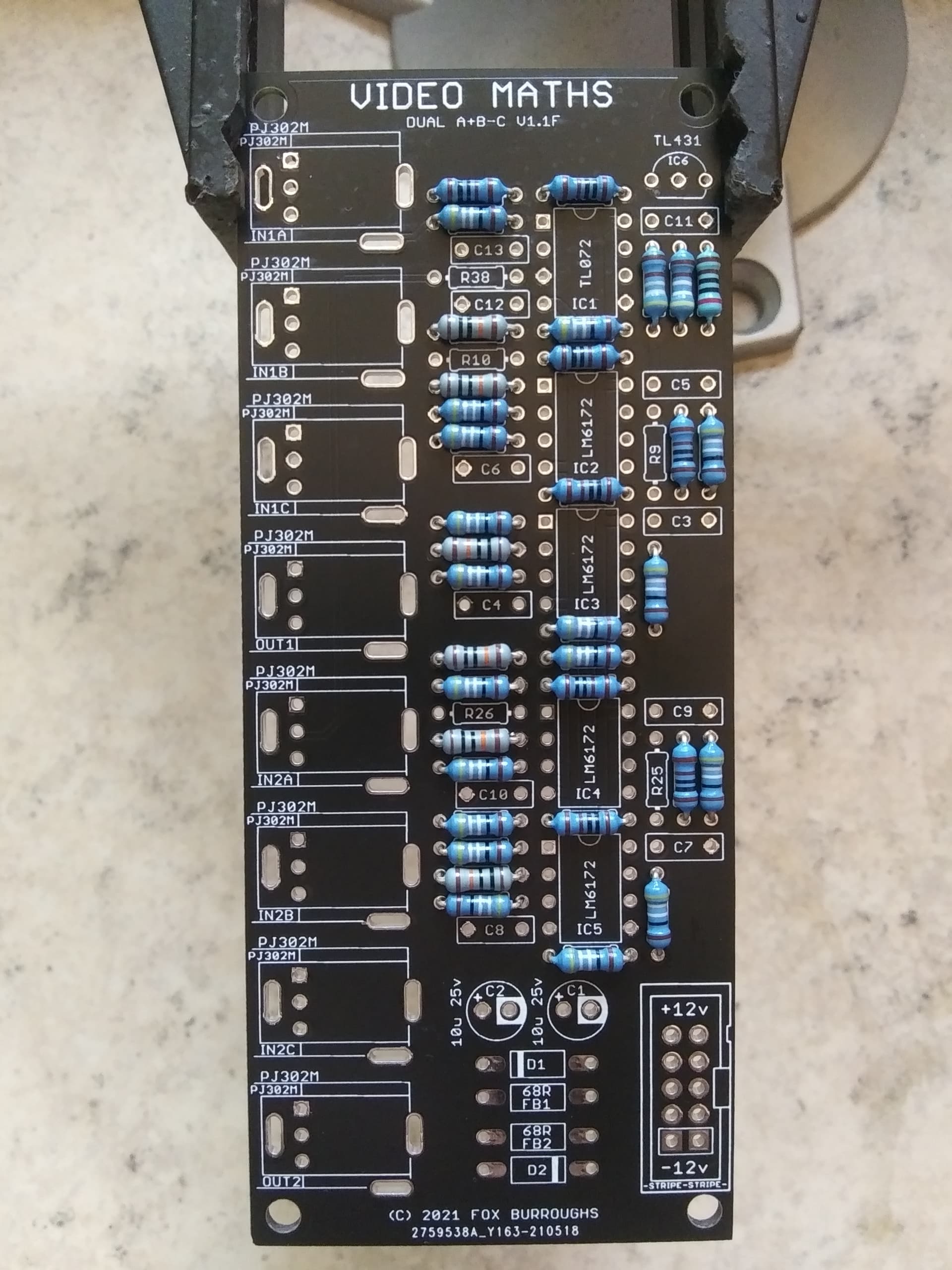
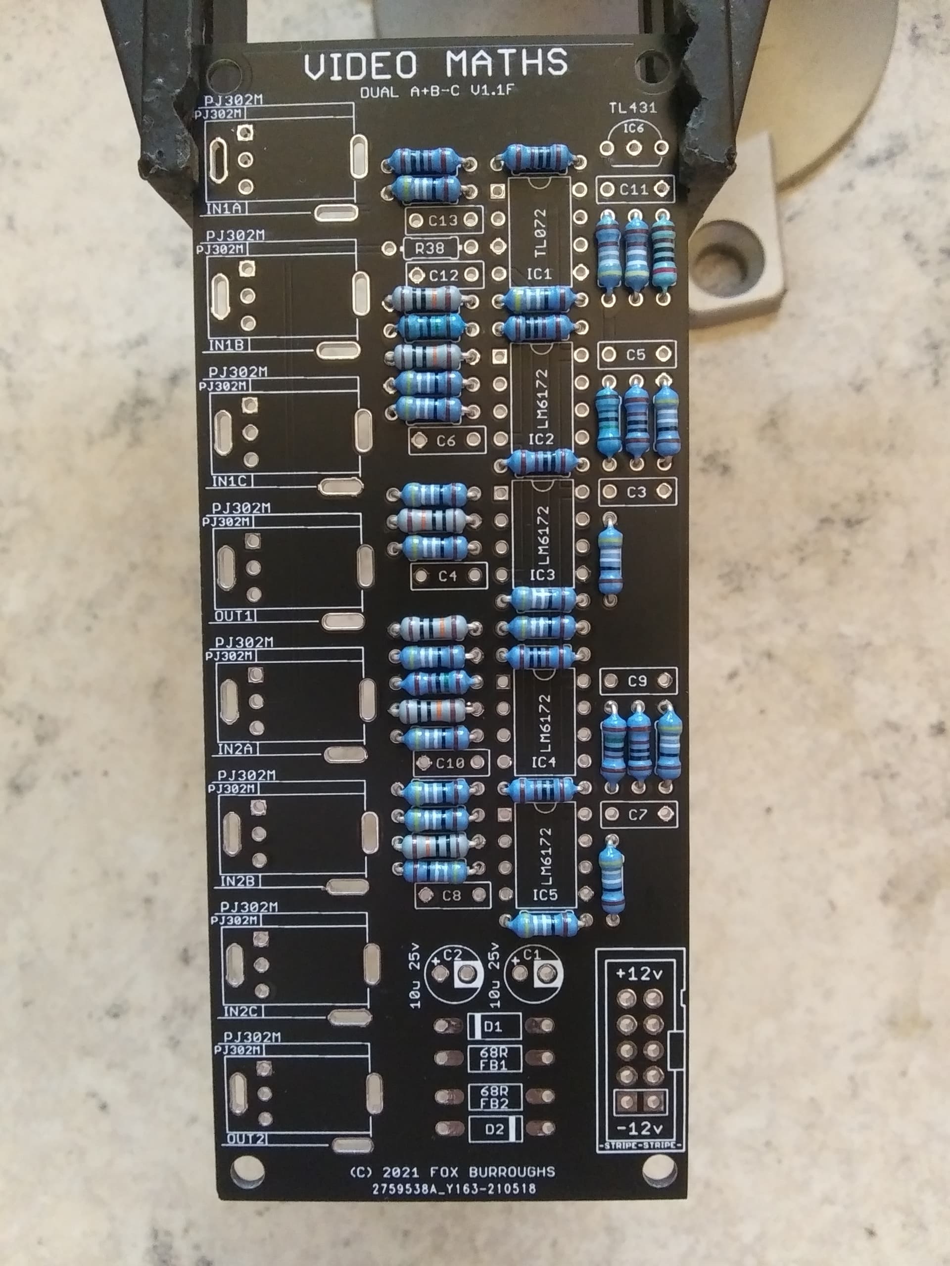
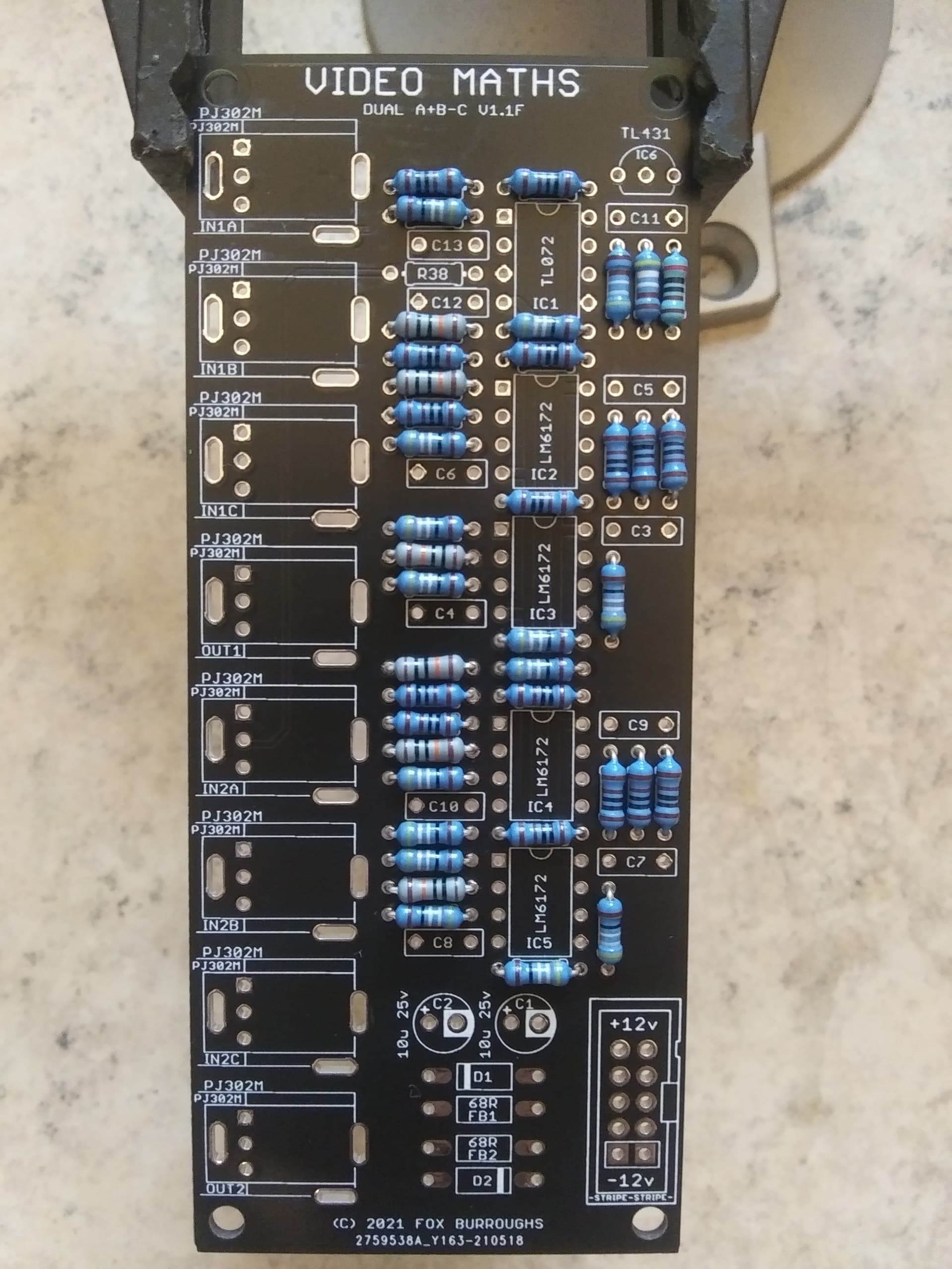
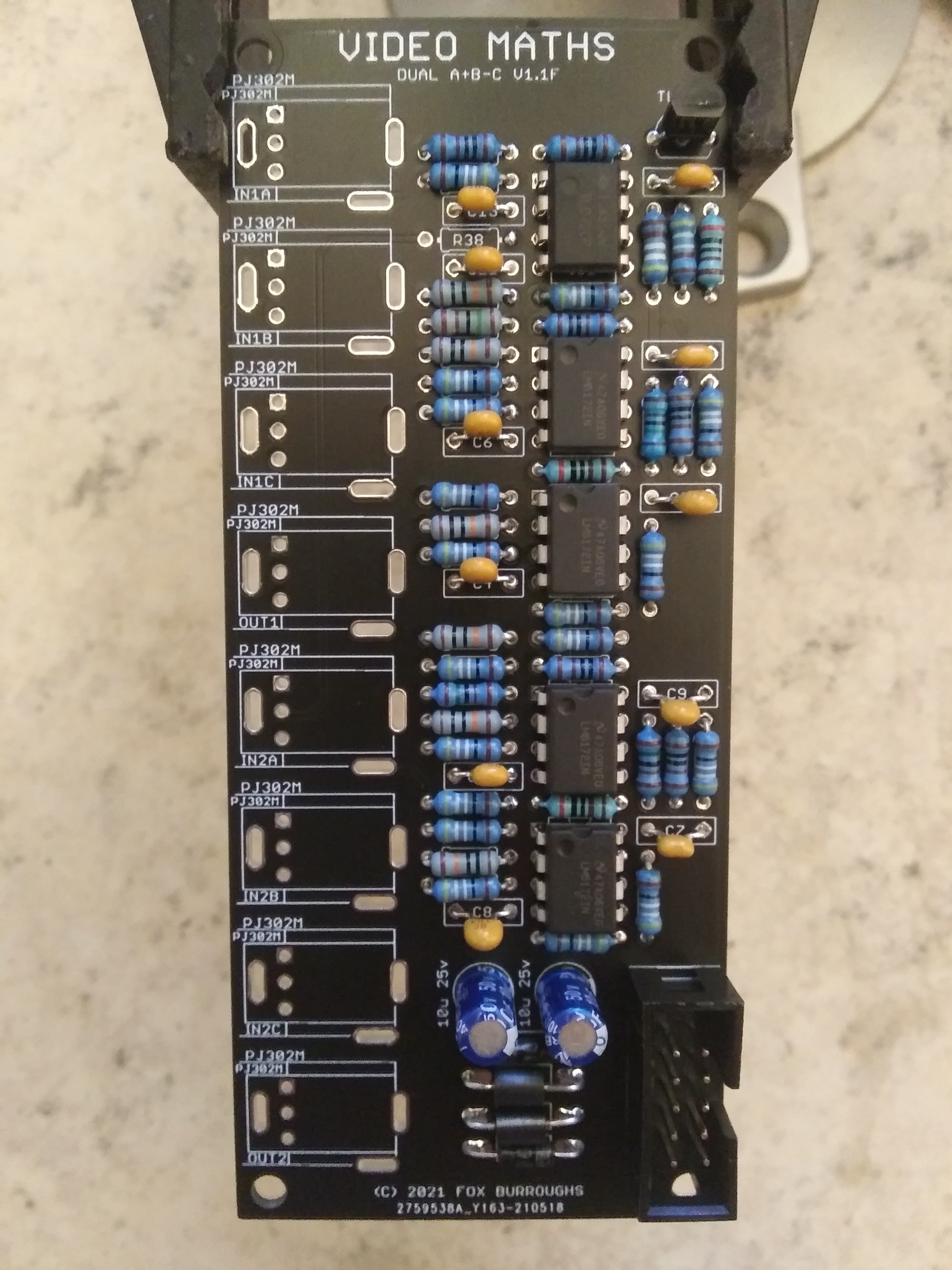
Start by populating the 499R resistors. There are 18 of them: R4, R5, R6, R7, R8, R13, R15, R16, R20, R21, R22, R23, R24, R29, R31, R32, R39, R42.
Step 2.
Next, populate the six 1K resistors: R11, R12, R27, R28, R36, R37.
Step 3.
Now populate all four 1.5K resistors: R9, R10, R25, R26.
Step 4.
Next populate all three 2K resistors: R14, R30, R35.
Step 5.
Finally, populate all six 100K resistors: R1, R2, R3, R17, R18, R19.
Step 6.
Now populate all eleven 100nF capacitors.
Step 7.
At the bottom of the board, populate both diodes and ferrite beads. Take note of the diodes polarity stripes. These line up with the lines on the pcb.
Step 8.
In the top right, populate the TL431.
Step 9.
The first op amp, IC1; is a TL072. Make sure pin 1 is inserted into the square via.
Step 10.
The other four op amps are all LM6172’s. Make sure pin 1 of each of them is inserted into the square vias.
Step 11.
Now populate the 10-pin shrouded header. The notch faces outward.
Step 12.
Now populate both 10uF electrolytic capacitors. These are polarized, so line up the stripe on the cap with the circled-via on the pcb.
Step 13.
There are eight PJ302M jacks. Place each of them into the board and install the faceplate carefully. Finger-tighten a nut onto each jack and make sure they are lined up straight before soldering.
Step 14.
Finally the last step is to add solder blobs to the jumpers on the bottom of the board. For this configuration, solder JP1 and JP3.
Thats it. Clean up your board and test!
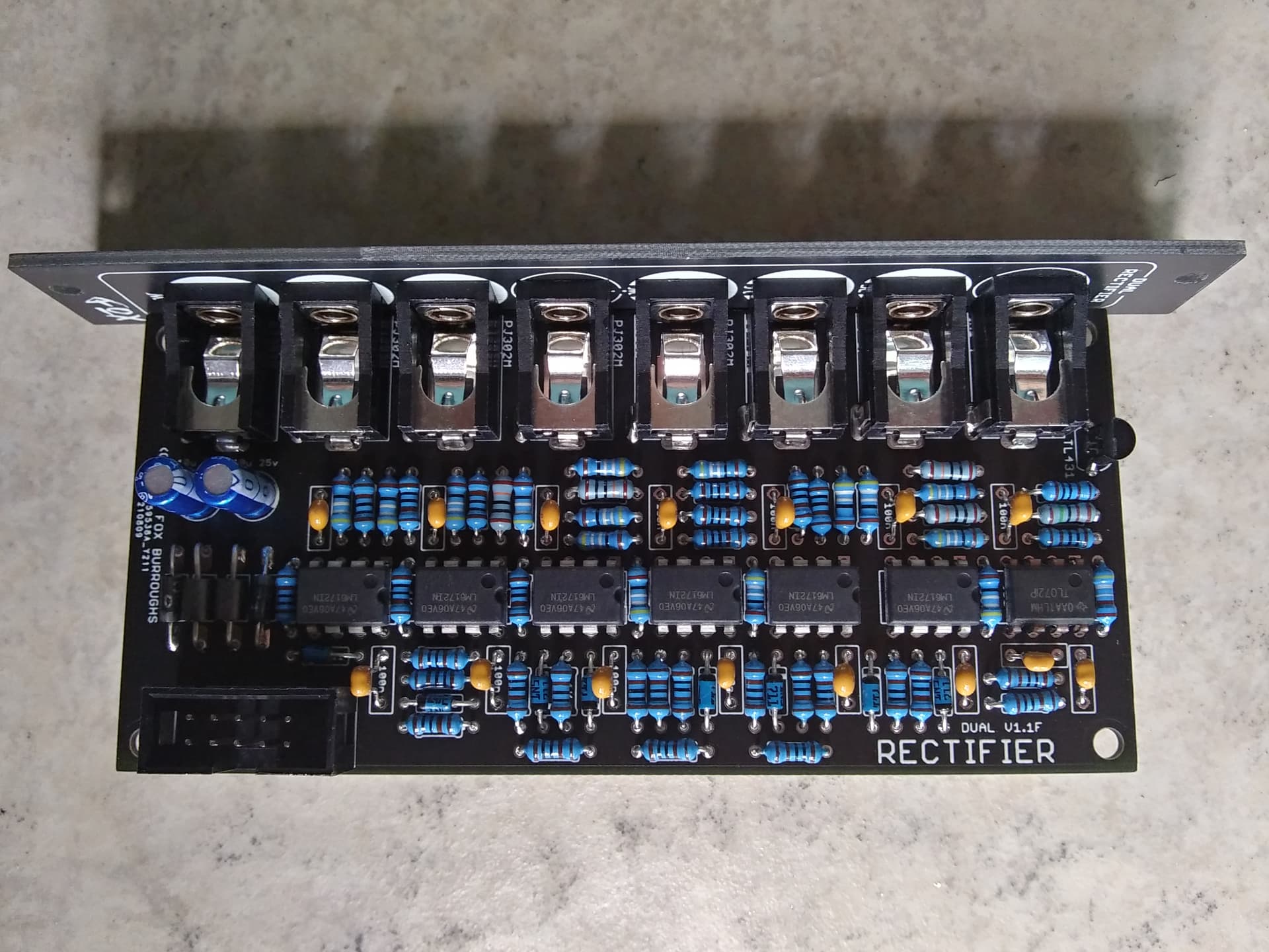
BOM for Rectifier
| Qty | Value | Parts |
|---|---|---|
| 1 | 1.5K resistor | R2 |
| 1 | 10-Pin Box Header | J9 |
| 4 | 100K resistor | R6, R8, R30, R32 |
| 15 | 100n capacitor | C3, C4, C5, C6, C7, C8, C9, C10, C11, C12, C13, C14, C15, C16, C17 |
| 2 | 10u 25v capacitor | C1, C2 |
| 31 | 1K resistor | R3, R4, R5, R10, R12, R13, R14, R15, R16, R17, R18, R20, R21, R22, R23, R24, R25, R34, R36, R37, R38, R39, R40, R41, R42, R44, R45, R46, R47, R48, R49 |
| 2 | 1N4001 diode | D1, D2 |
| 1 | 4.99K resistor | R1 |
| 15 | 499R resistor | R7, R9, R11, R19, R26, R27, R28, R29, R31, R33, R35, R43, R50, R51, R52 |
| 8 | 1n5711 diode | D3, D4, D5, D6, D7, D8, D9, D10 |
| 2 | 68R ferrite bead | FB1, FB2 |
| 6 | LM6172 op amp | IC3, IC4, IC5, IC6, IC8, IC87 |
| 8 | PJ302M jack | BOTTOM1, BOTTOM2, FOLD1, FOLD2, IN1, IN2, TOP1, TOP2 |
| 1 | TL072 op amp | IC2 |
| 1 | TL431 reference | IC1 |
| 8 | nuts | - |
| 1 | Pcb set | - |
| 1 | 10-16 ribbon cable | - |
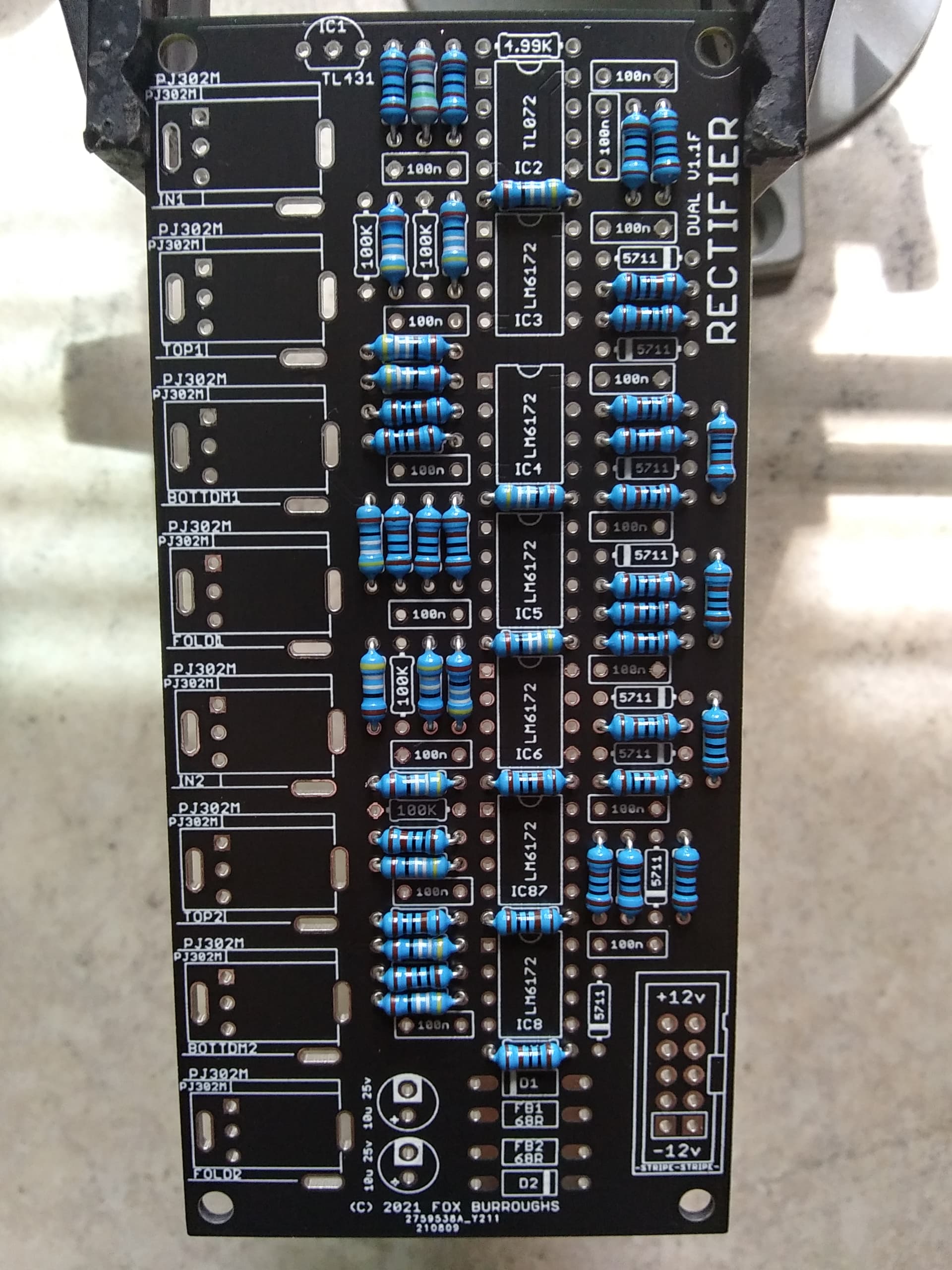
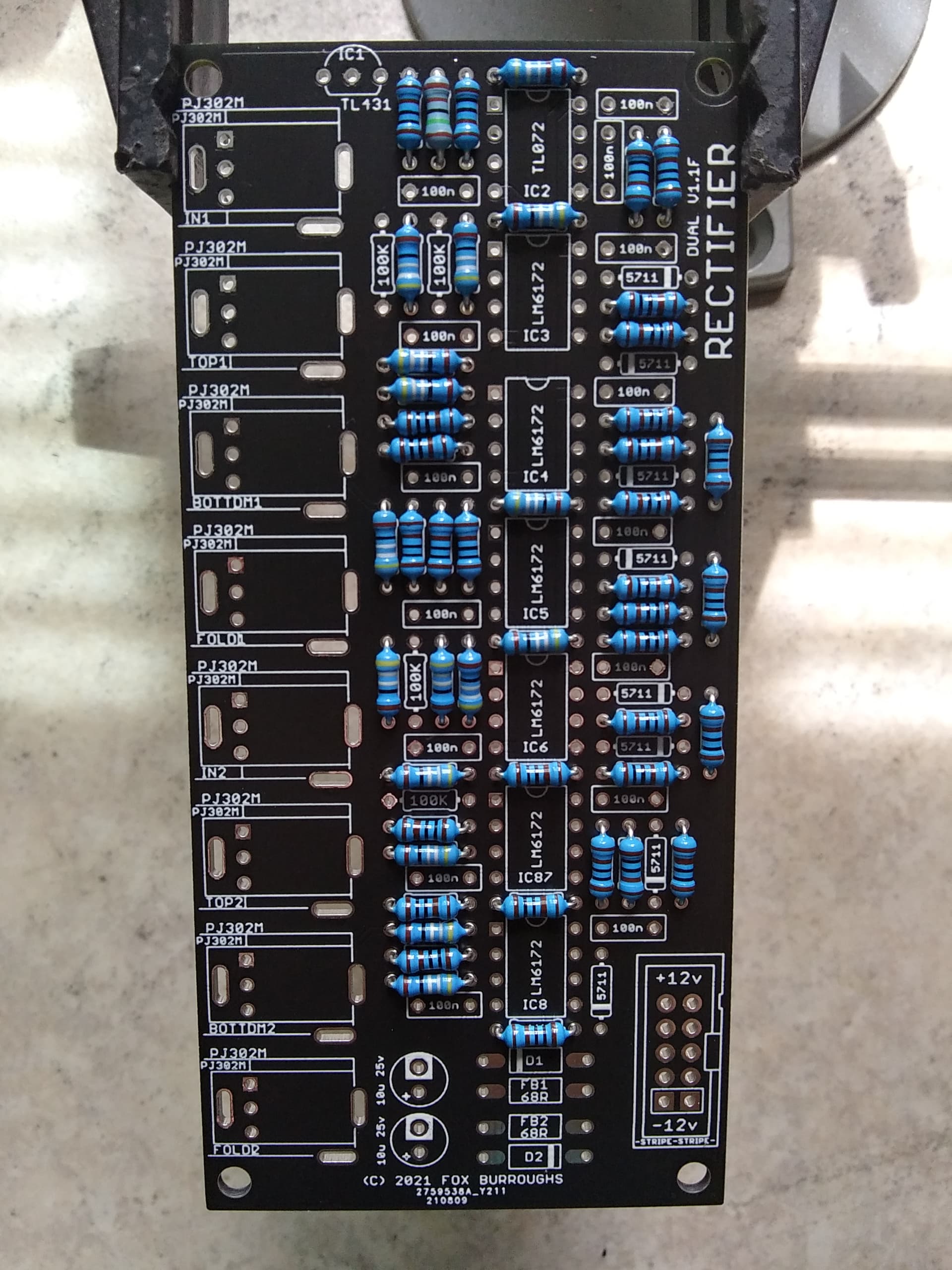
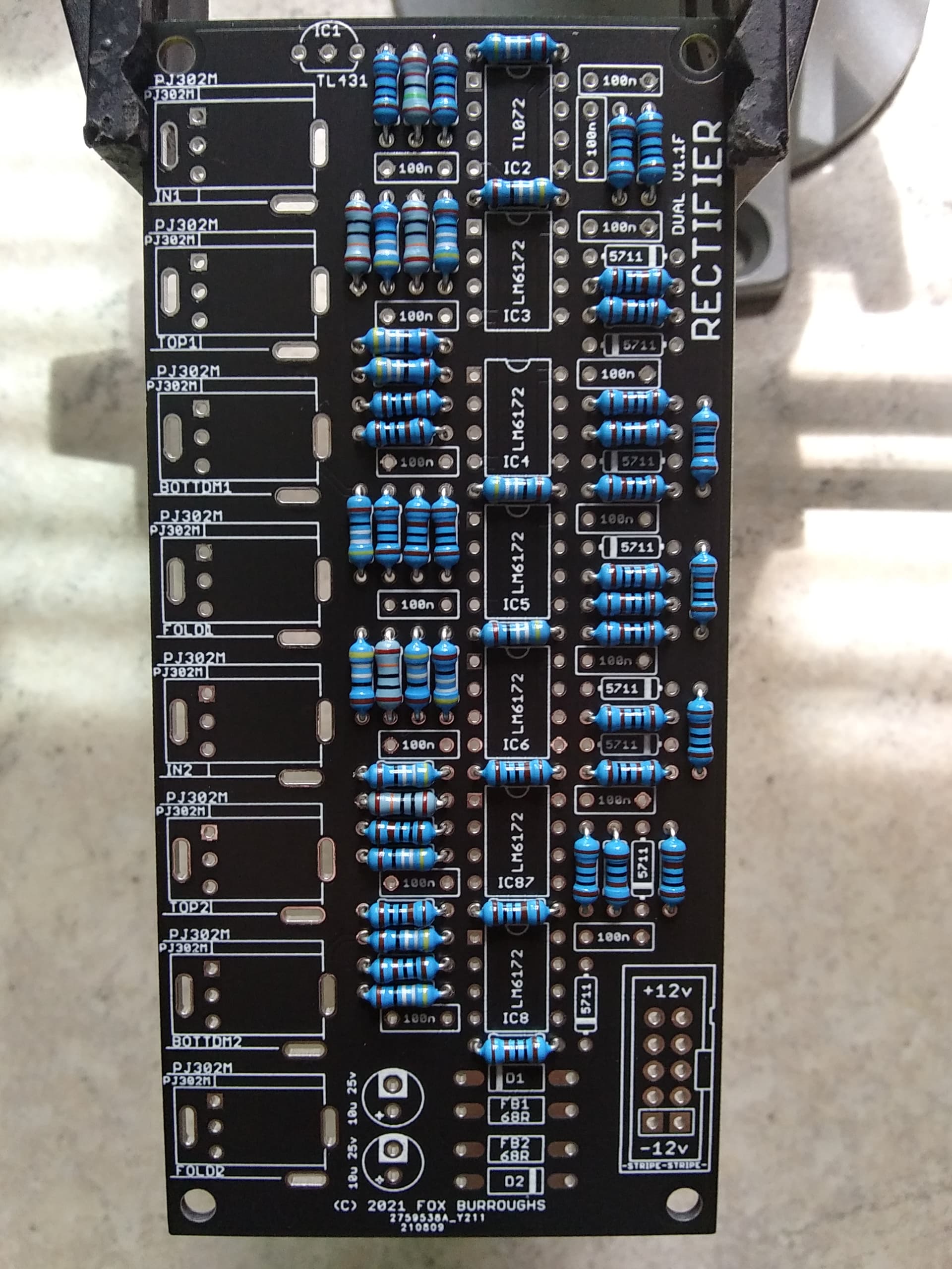
Build Guide for Rectifier
Step 0.
Using a PCB vice will improve your DIY experience immensely. I’ve been using the same Panavise Jr. since 2014.
Step 1.
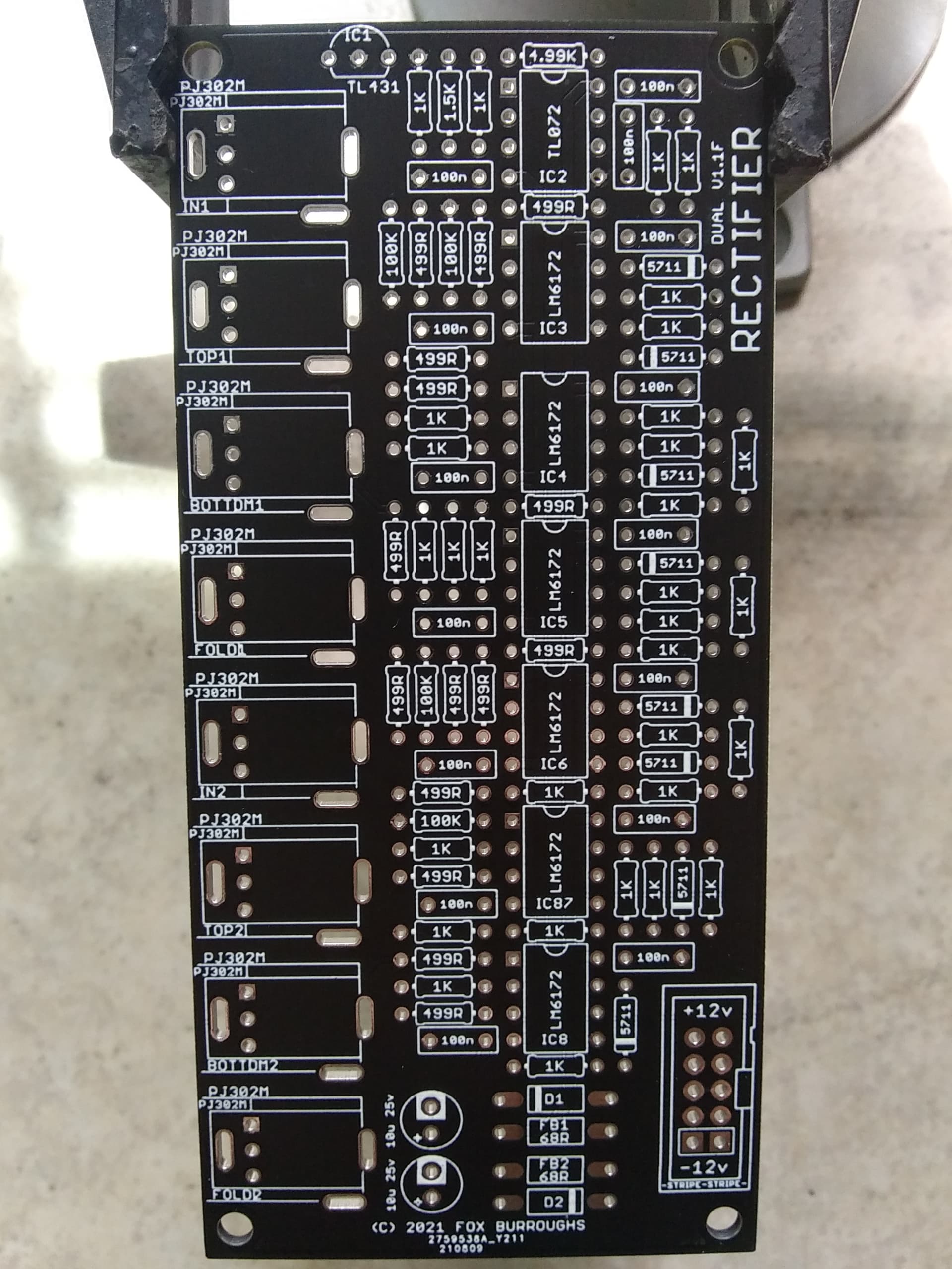
Start with the fifteen 499 ohm resistors.
I prefer to populate all of the resistors at once, and then solder them in place.
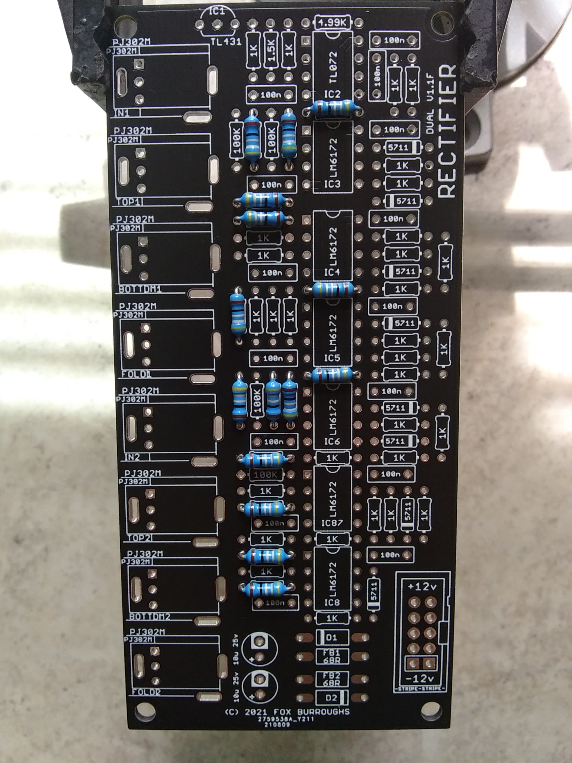
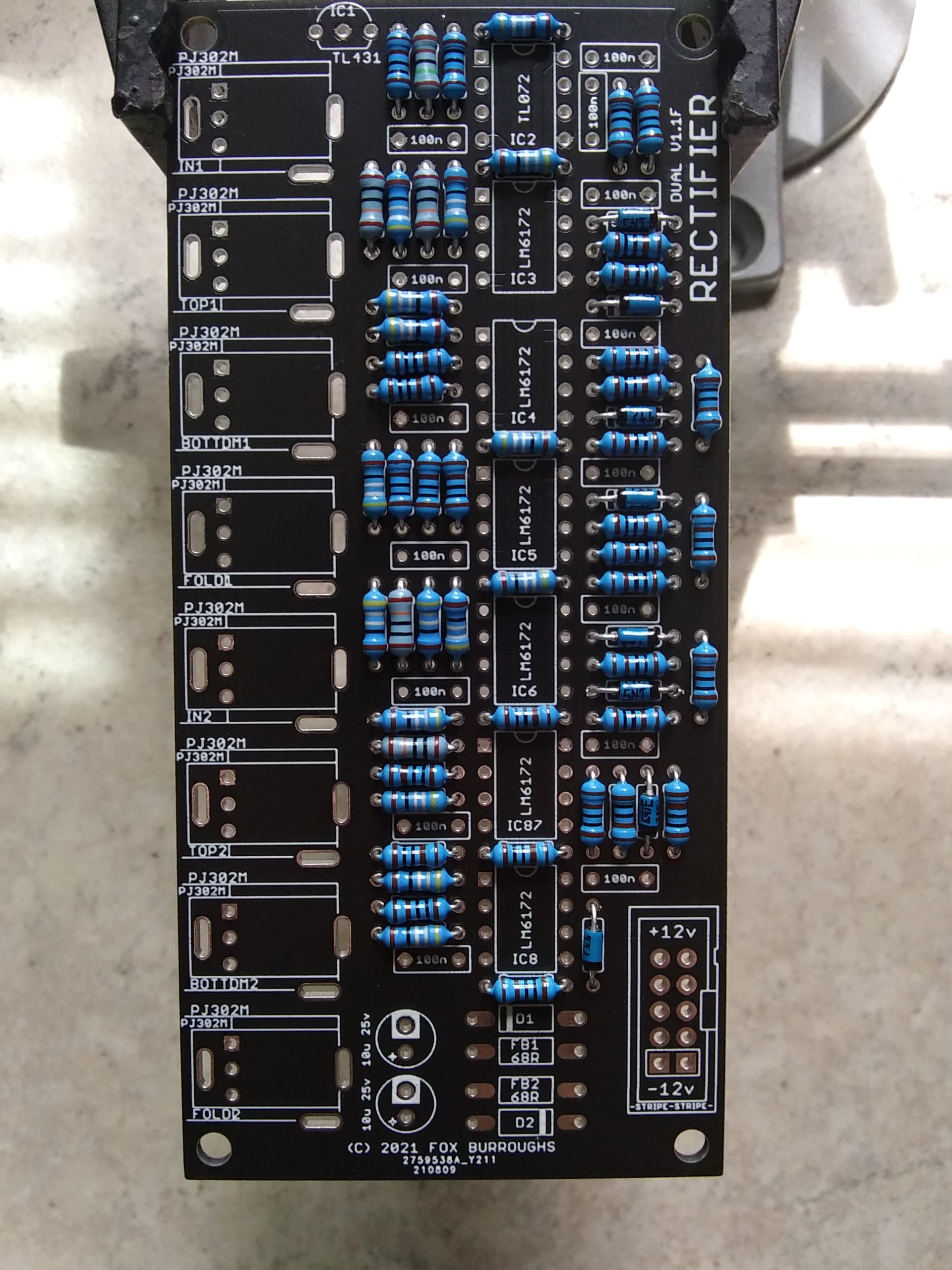
Step 2.
Next we will populate the 1K ohm resistors. There are a whopping 31 of them!
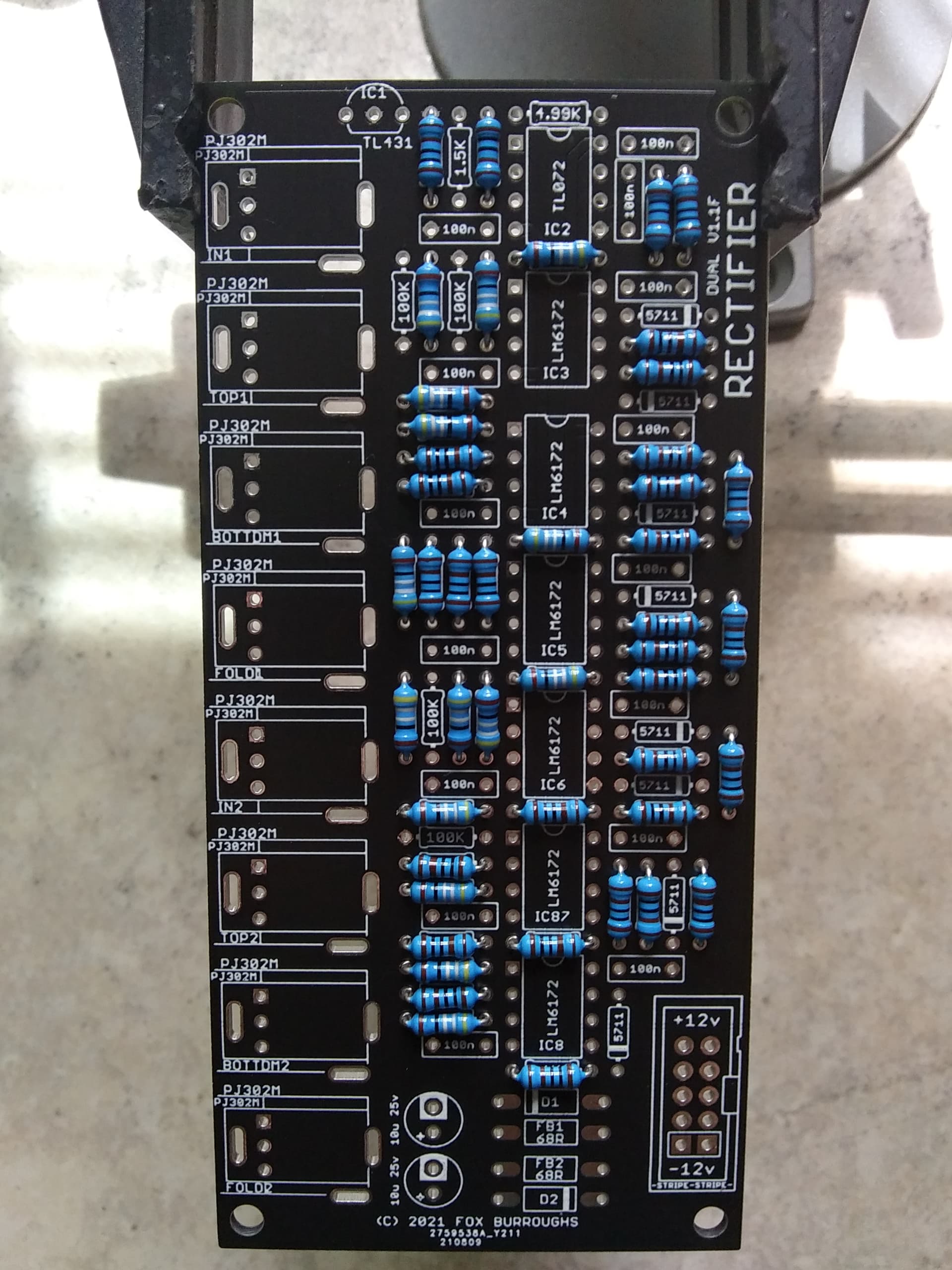
Step 3.
At the top, there is a single 4.99K ohm resistor and a single 1.5K ohm resistor. Populate both of them in their respective locations.
Step 4.
Next, populate the 100K ohm resistors. There are only six.
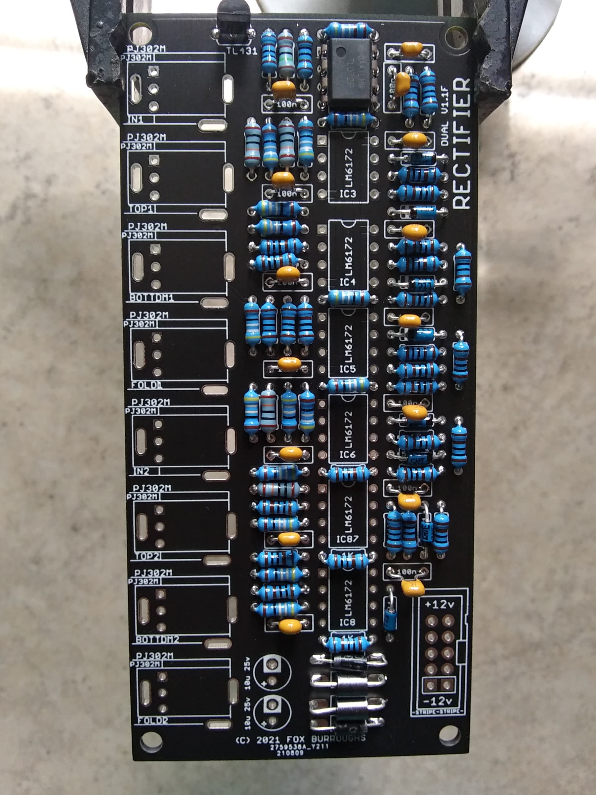
Step 5.
Now we have to add the 1n5711 diodes. Take note, these are polarized. Make sure the stripe on the diode matches the same direction as the stripe on the PCB. There are 8 diodes.
At this point, I carefully flip the board over onto my workspace and solder each leg then clip them all.
Step 6.
Now we can add both ferrite beads and both protection diodes. The ferrite is not polarized, but the diodes are. Line up your diodes properly and then solder all four parts in place. Clip the legs.
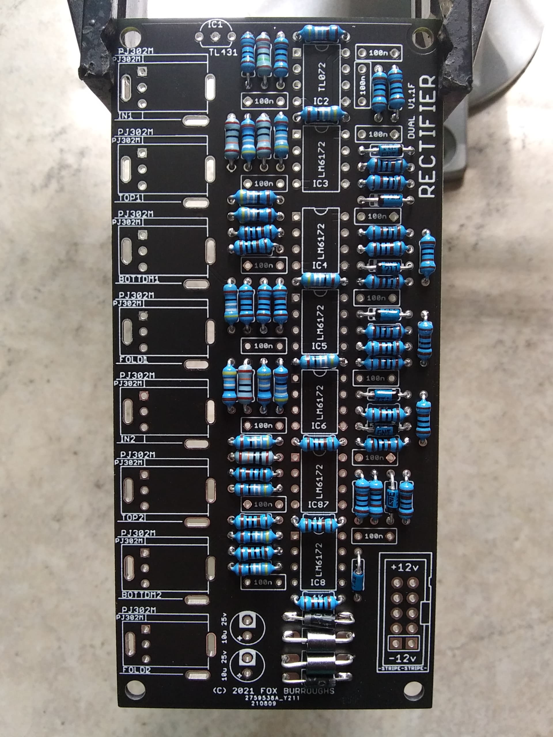
Step 7.
Now we can add all fifteen of the 100nF caps. Solder and clip.
Step 8.
Now place your TL431 voltage reference. It is located at the top of the board.
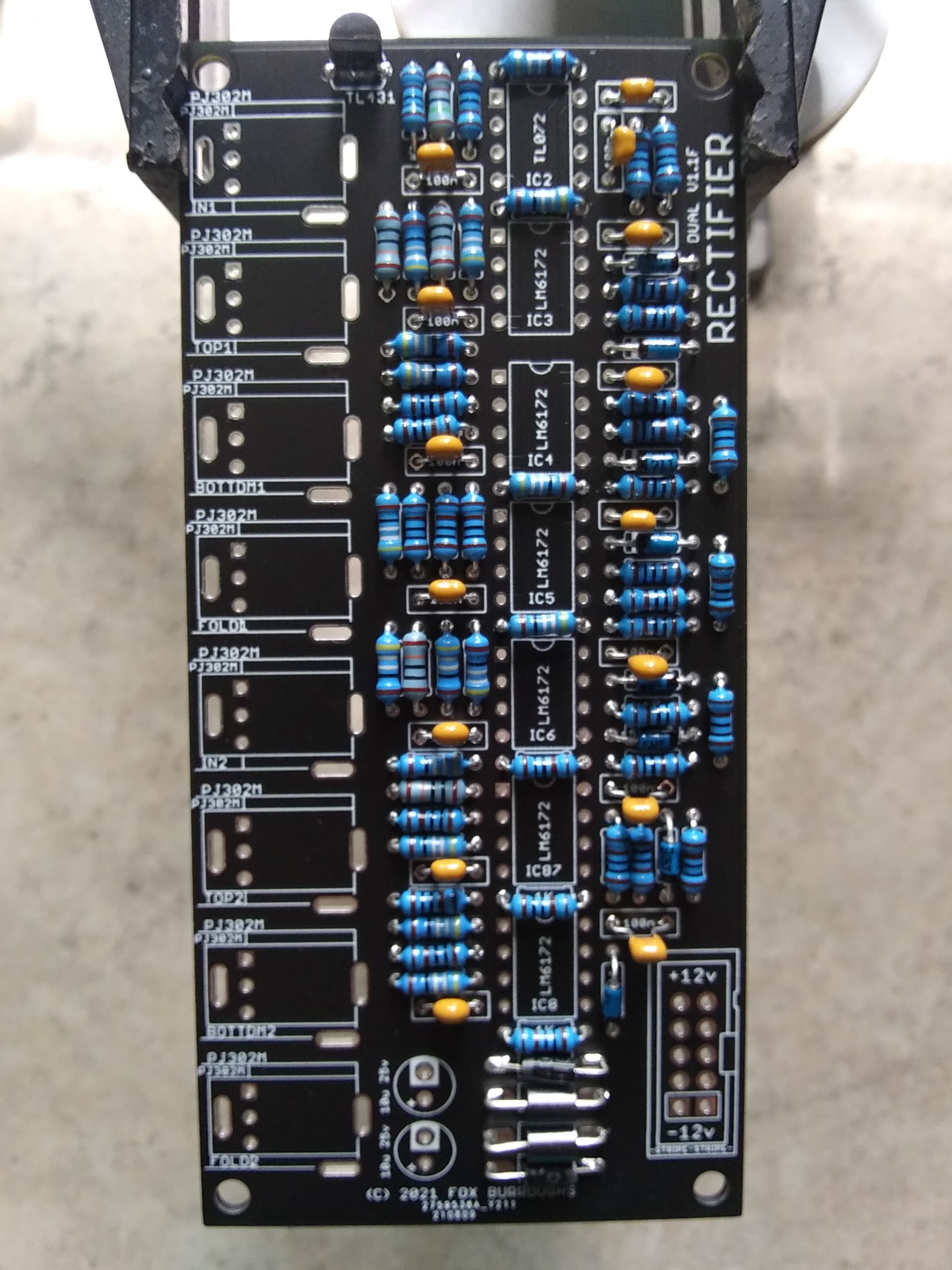
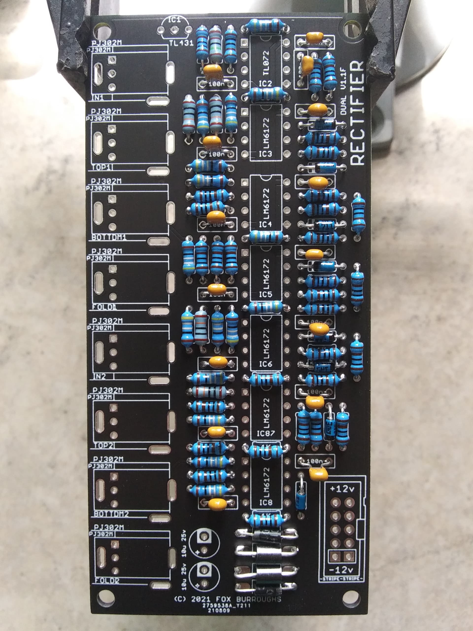
Step 9.
Here we will add all of our op amps. The top-most IC is a single TL072 while the remaining six are all LM6172’s. Make sure pin 1 of each IC is placed into the square hole.
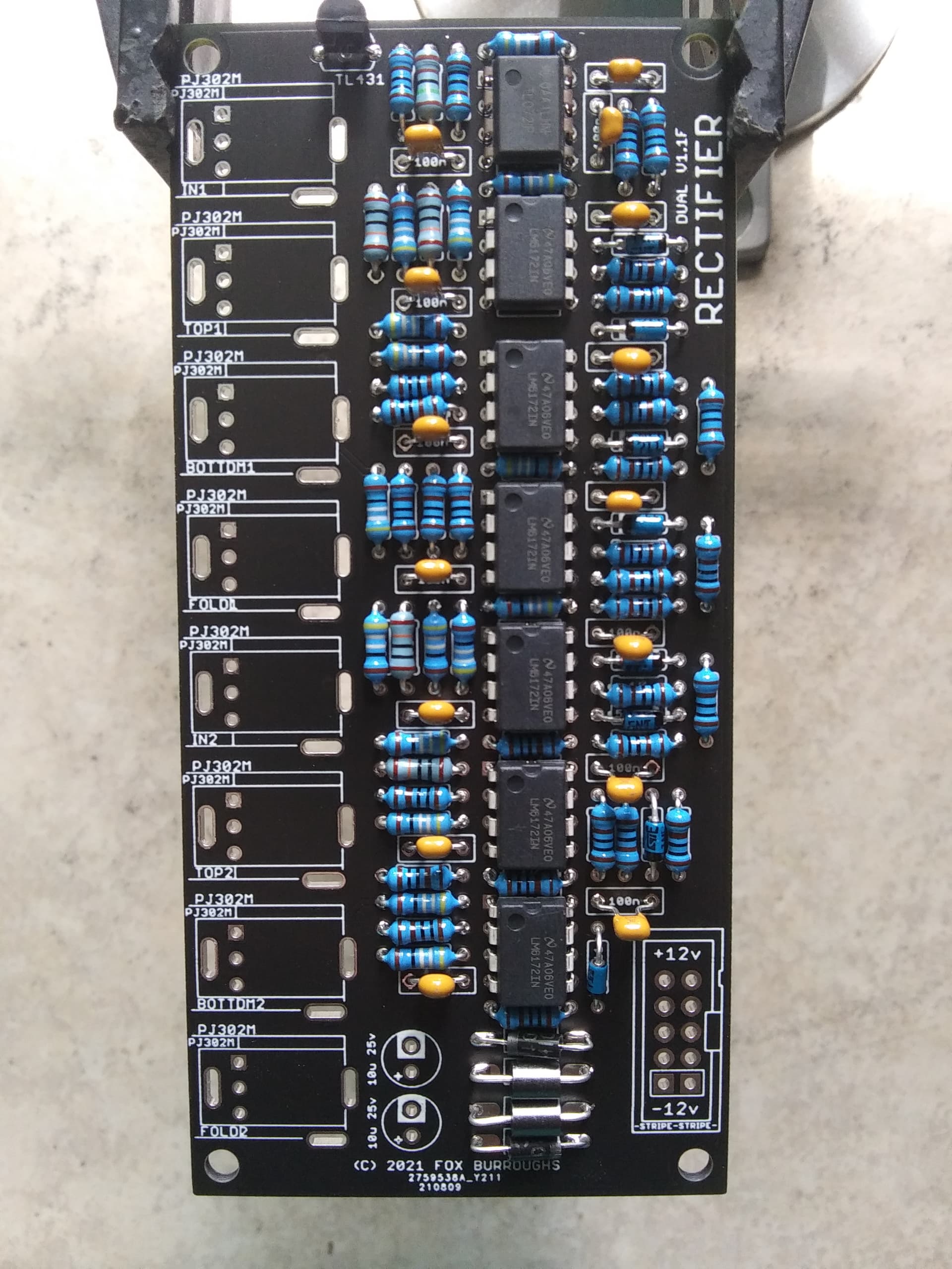
Step 10.
Here we will add the 10-pin box header.
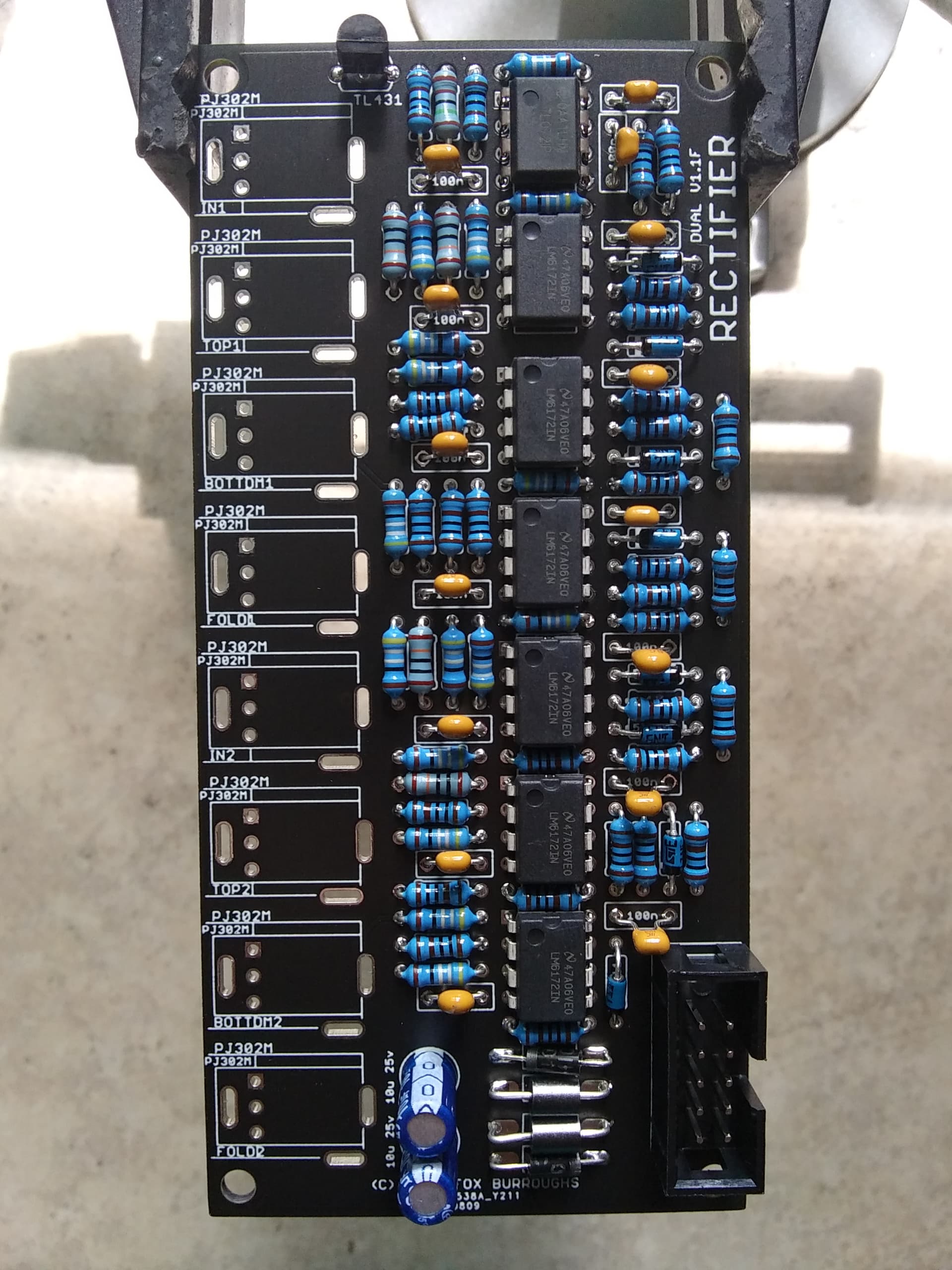
Step 11.
Place all eight of your PJ302M jacks in place and carefully install the faceplate before soldering. The faceplate is reversible so you may choose whichever side suits you.
Finger-tighten a nut onto each jack and make sure they are lined up straight. Once they are, you may solder them in place.
At this point, it is a good idea to use some isopropyl alcohol and a tooth brush to clean the bottom of your board and remove any crusty solder flux. Once it is clean, take a good long look for any solder blobs or cold joints. Fix as necessary and test. Enjoy!