I use Cadet modules for I/O on my system and recently added S-Video output to my Cadet II in place of the PAL/NTSC switch which has worked well.
I’d like to move on up to component output and after researching a bit, I think I’ve found a schematic I could reasonably adapt to add component to Cadet II. I know just enough about electronics to get into trouble so I wanted to ask if anyone had some pointers before I whip up a protoboard.
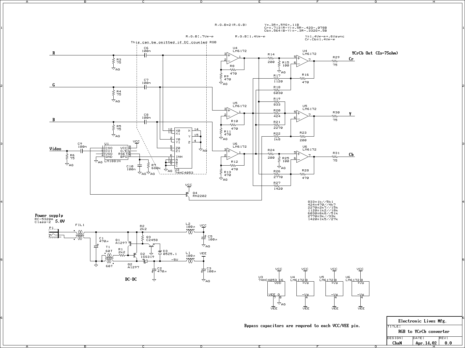
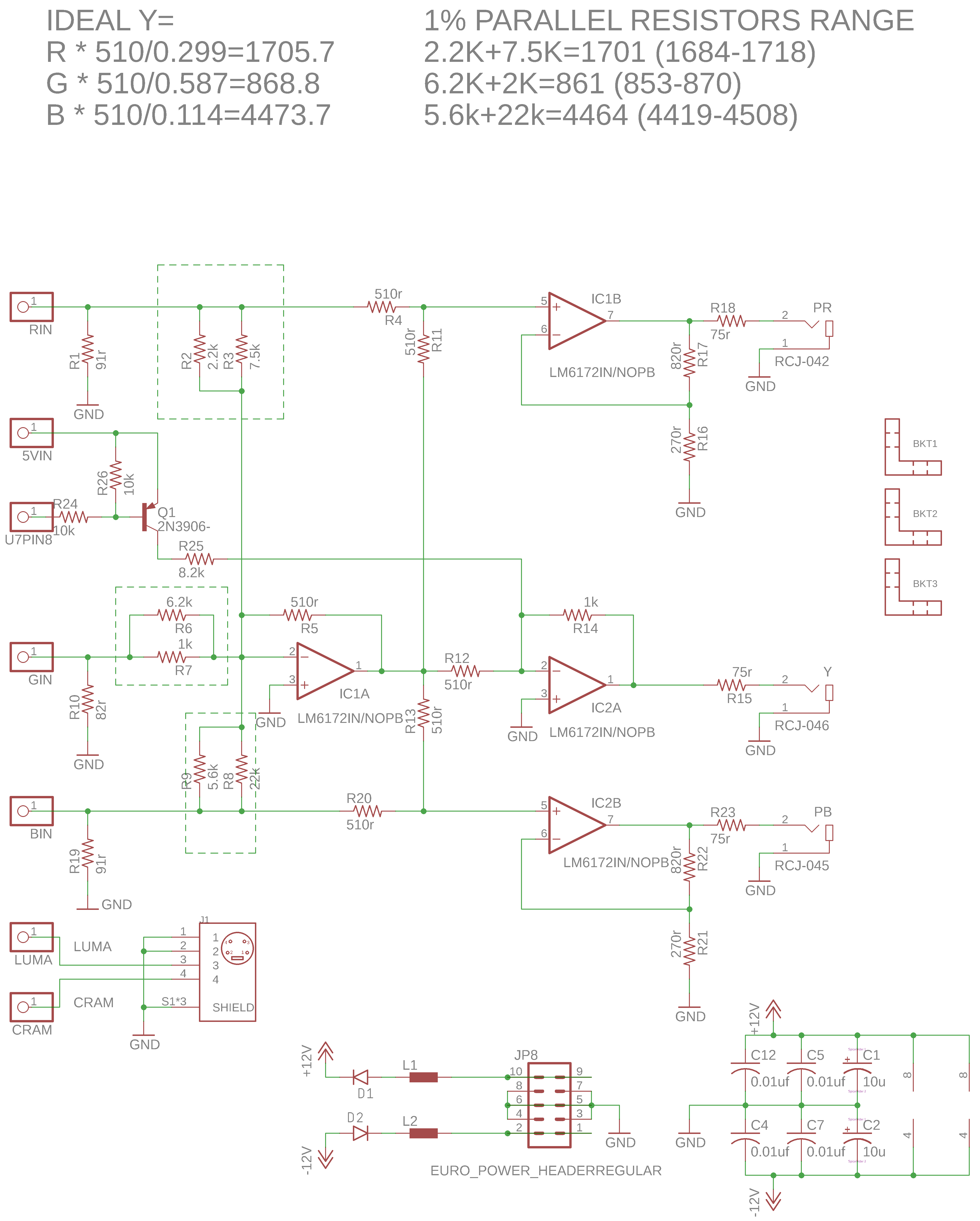
Would I be able to simply tap the Cadet II’s RGB lines that go into pins 6-8 on the AD724 before C12, C13 & C14 and put them into the RGB to YPbPr schematic below starting at the non-inverting input pins of the 3 LM6172s (skipping the input 75 ohm resistors and CD4053 stage)?
For sync insertion onto the Y channel thru Q4, could I tap the CSync pin from the Cadet II’s sync header instead of having the LM1881 in there?
I’m not 100% certain, but I think what you’re proposing will work (as long as the rgb-to-ypbpr schematic is good). I think it’s definitely worth a try to see how well it works. The only thing I can foresee maybe being an issue is the gain on the leftmost LM6172’s in the rgb-to-ypbpr, but that’s only because I’m not quite sure what level is coming out of the black and white level clippers in the Cadet2. Though based on the input specs in the AD724 datasheet, it seems like it should be the 0.7p-p level mentioned in the rgb-to-ypbpr schematic, so it’s probably exactly right! And even if the gain were a little off, that’d be easy enough to fix by changing the relevant resistors there.
Out of curiosity, are you planning on making a separate LZX-to-YPbPr module out of this? Or is it going to be an expansion to the Cadet2?
Wonderful, I’m glad it doesn’t look like I’m completely off base here. I’ll try to solder something up soon to see if it works and share that here.
I noticed that they noted the voltage level on the RGB to YPbPr schematic and from Lars’ response on this thread about the Cadet II clipper circuit, it seems to pretty much match up with the expected voltage level.
My initial idea was to tack this circuit onto my Cadet II and install the YPbPr jacks in an adjacent 4HP blank or on a 1U row right below it. If this turns out to be right (or if it’s too noisy on protoboard), I’d be up for working with someone who knows PCB layout better than me to produce a 8HP layout with YPbPr built into it.
I also think you’re on the right track. Lars’ 0-1V clipper is one of my favourite circuits, it’s so incredibly useful! You will most likely find this works OK on breadboard - I have made lots of circuits like this and they’ve generally worked just fine. The best way to find out the answers to all your questions is to try it out! It’s fun and nothing beats practical learning.
Awesome, appreciate the offer! I got it mostly working on the breadboard yesterday so I anticipate it won’t take too long to iron out the kinks.
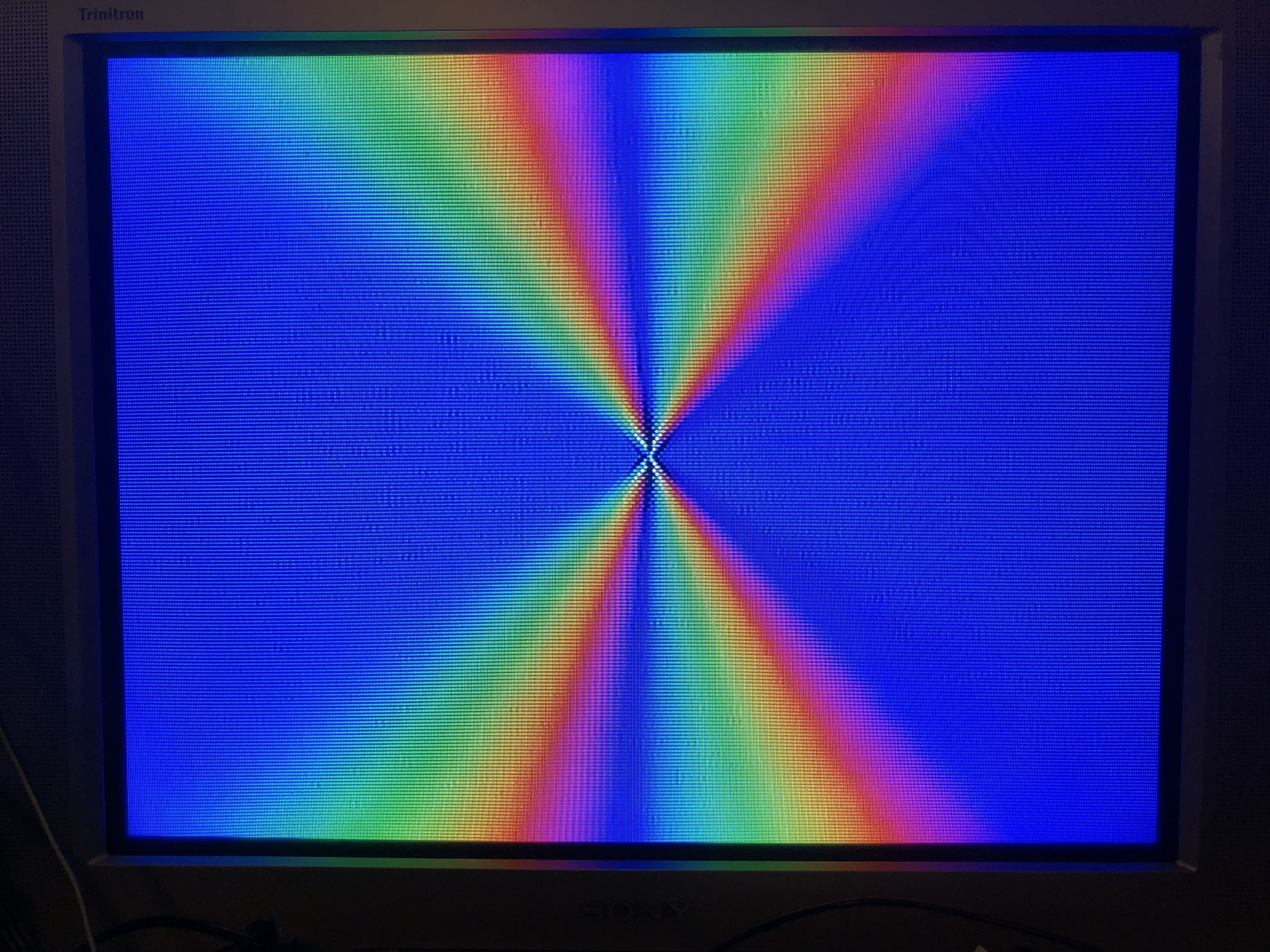
Currently all three of the component outputs are sending a valid signal and sync is working but the colors look a little off and there’s a small horizontal smear at the top of the screen. I’m going to throw it onto a stripboard to see if that helps at all and will post an update from there.
Had a quick study of the cadet II schematic again and a reread of the posts here. Where are you tapping CSync from? Sync signals come into the header and are buffered by inverter U7. If you are taking your RGB from pins 6-8 of AD724, the blanking signal has been inverted twice. You need to take Csync after U7 too otherwise the blanking signal will be slightly behind where it should be. U7.4 output is pin 8. This might be the cause of your issue
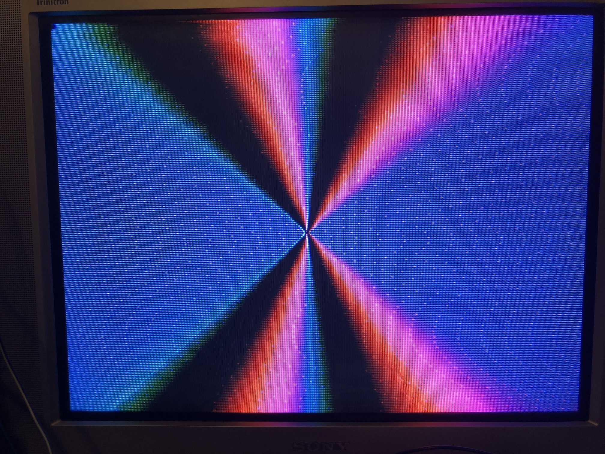
Ah, that makes more sense–thanks! I went ahead and swapped where I was tapping CSYNC from pin 14 of the sync header over to pin 8 of U7 and that did help clear up most of the horizontal smear I had at the top of the screen.
The color is still looking funky, though. Here’s a quick photo from the Cadet II composite output vs. the component output with the same patch. I’m not certain if the wavy lines are the result of breadboard noise or an error with my layout.
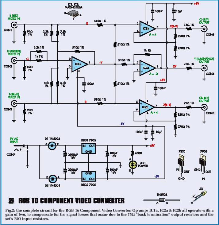
I did find another RGB to YUV schematic online but it uses MAX4451s that I don’t have on hand. Not certain if LM6172 is a drop-in replacement for it or requires tweaking.
I will have more of a think about this, but I think that may be a timing issue also. I zoomed in closely to the second image. There is a pixel that is too bright at regular intervals.
That second circuit, maybe I am blind but where is the sync signal injected?
That photo looks like it’s missing green from the output but its in there somewhere because it’s bright enough to suggest that you’re getting Y. What is your output going to? It’s way easier to just buffer the clipped and blanked RGB lines (and add sync to green if you need), bypass the NTSC encoder and then buffer the outputs if your next input can take RGB. I did this and put a switch to send sync to all three outputs so it could also be used as 3 monochrome outs.
The Cr calculation at the top of the rgb2yuv schematic are at odds with the one at https://en.wikipedia.org/wiki/YCbCr (scroll to ITU-R BT.601 conversion) but it’s not off by enough to do what’s happening in your photo. I built a syncless converter with eurorack input and output impedances using the basic topology from that schematic but doing the math from scratch and it worked well, so I’m guessing it’s a build error, flakey breadboard, or something wrong with the sync insertion into Y.
I agree with @gzifcak about the absence of green. The small amount of green smearing could easily be related to that - an unwired input picking up stray signal electromagnetically or similar.
MAX4451 op-amps would be near enough to interchangeable (they are a lower voltage part than the LM6172 though, so the reverse doesn’t apply). I’d experiment with resistor values and/or do your own calcs like gzifcak did.
The curvy dots might be from a switch mode power supply or some other nearby oscillator? Maybe try swapping to a linear supply if you have one, but that’s just a guess, something to check out. Try disconnecting/re-connecting the Cr and Cb inputs to see if you can work out which signal line it is on, that might give you some more info to work with.
I don’t own a display that accepts component in here. Need something for hooking up some old games consoles to the new TV anyway, so I am buying a cheap component to HDMI converter box. This means I can build the same circuit as you at home and help figure this out. I want to make PCBs of these so need to test anyway.
The second circuit has the resistor scaling within margin of error of the ITU-R BT.601 conversion, I would base it off that circuit plus its fix. I am 99% certain you will need Q1 and its 3 resistors between pin 8 of Cadet II’s U7 to pin 2 of IC2A. The fix sums an inverted Y with an inverted sync in an inverting opamp, giving you non-inverted sync+Y. I think without Q1, you will get inverted sync+Y but I haven’t looked at the LZX sync bus with a scope yet. Values of the 3 resistors may need to change.
Thank you for the poke, I am up for this just not the greatest communicator. I am actually pretty far advanced with this, I have a schematic and a PCB layed out already just haven’t done anything on breadboard yet. I plan for an S-video jack on the PCB too. I might get round to some breadboard experiments in the next day or so.
I spoke a little soon about the resistor scaling. I have calculated correct values. I also think the gain of the 3 amplifiers to the right need to be unity (if I am right then R14, R16, R17, R21, R22 should all be 510r).
Oh yeah, also R1, R10 and R19 are just taken from the other schematic and likely not needed here. And if we change the gain of the 3 amplifiers to unity then R25 will probably need to be halved
Fantastic progress, thanks for sharing! For the S-Video output, you’ll need to add a 220uF cap and a 75 ohm resistor between the pads and the connector.