LZX Show & Tell, lzxpcb-fpga12 / ESG3 review

We thought some of you may enjoy seeing some behind-the-scenes action, so I’m going to try to post more on that topic.

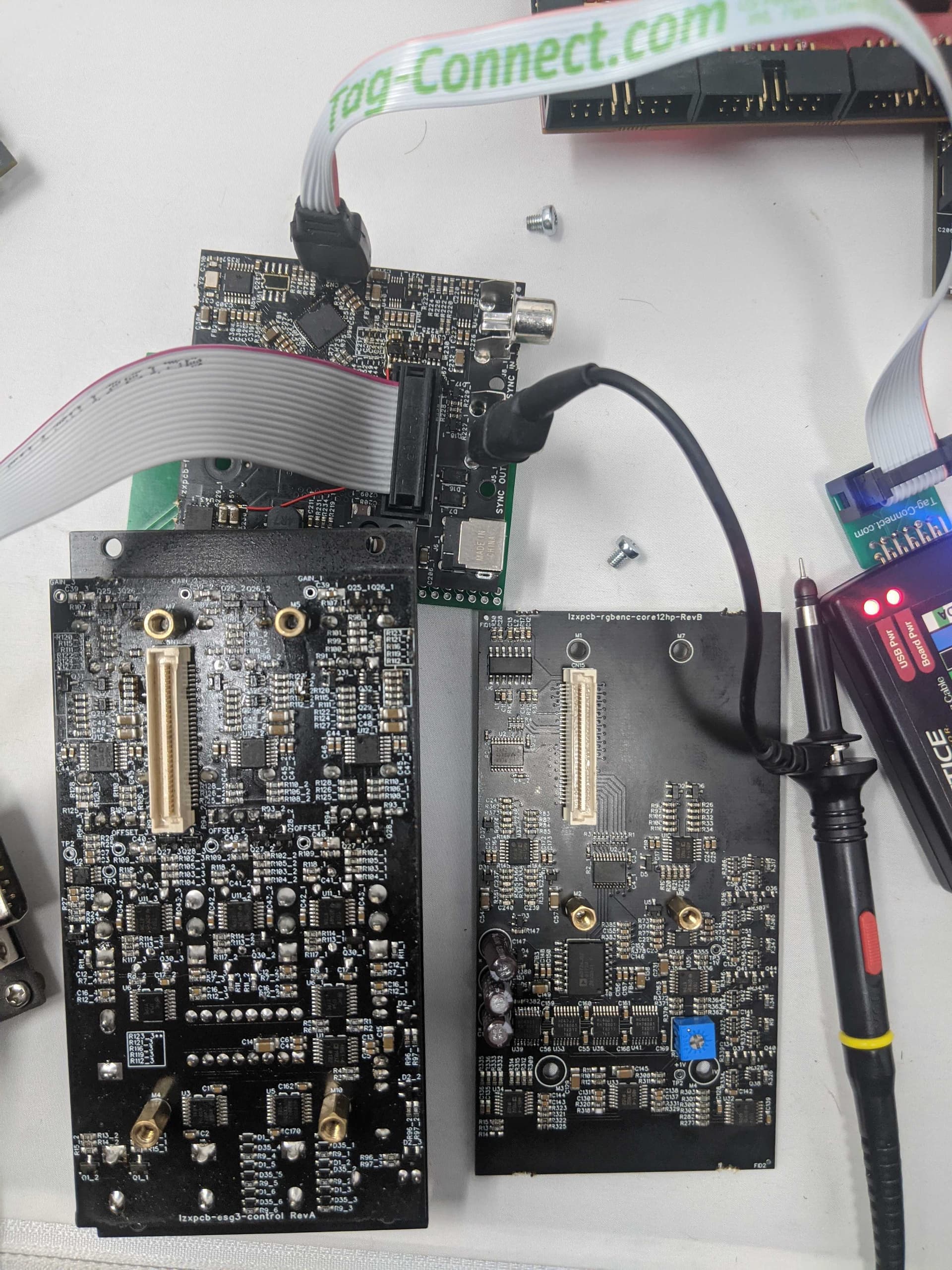
Today we reviewed a new PCB that came in last week, lzxpcb-fpga12hp-RevA The workshop team built 5 of these up yesterday. This is the third “outer layer” variant for Gen3, and is a general purpose power entry and FPGA subsystem PCBA. The first two modules that will use this assembly include ESG3 and DSG3.

This board is similar to our existing power entry + sync separator board (p/n lzxpcb-sync12), but adds an HD/SD Clock Generator and a small Lattice ICE5 series FPGA. In ESG3, this FPGA’s firmware is responsible for everything related to generating the timing of the video encoder’s outputs.

Another feature we like on this board is the Tag-Connect programmer footprint! We finally decided to give these spring-loaded pin cables a go since our footprint demands were so small on this board.

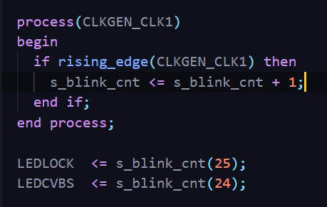
At the end of the day we’ve got our test articles all powering up, with firmware uploading successfully! With this confirmed, tomorrow we move on to testing our other new review board this week: lzxpcb-esg3-core. If that one looks good, we’ll be one big step closer to greenlighting this project.

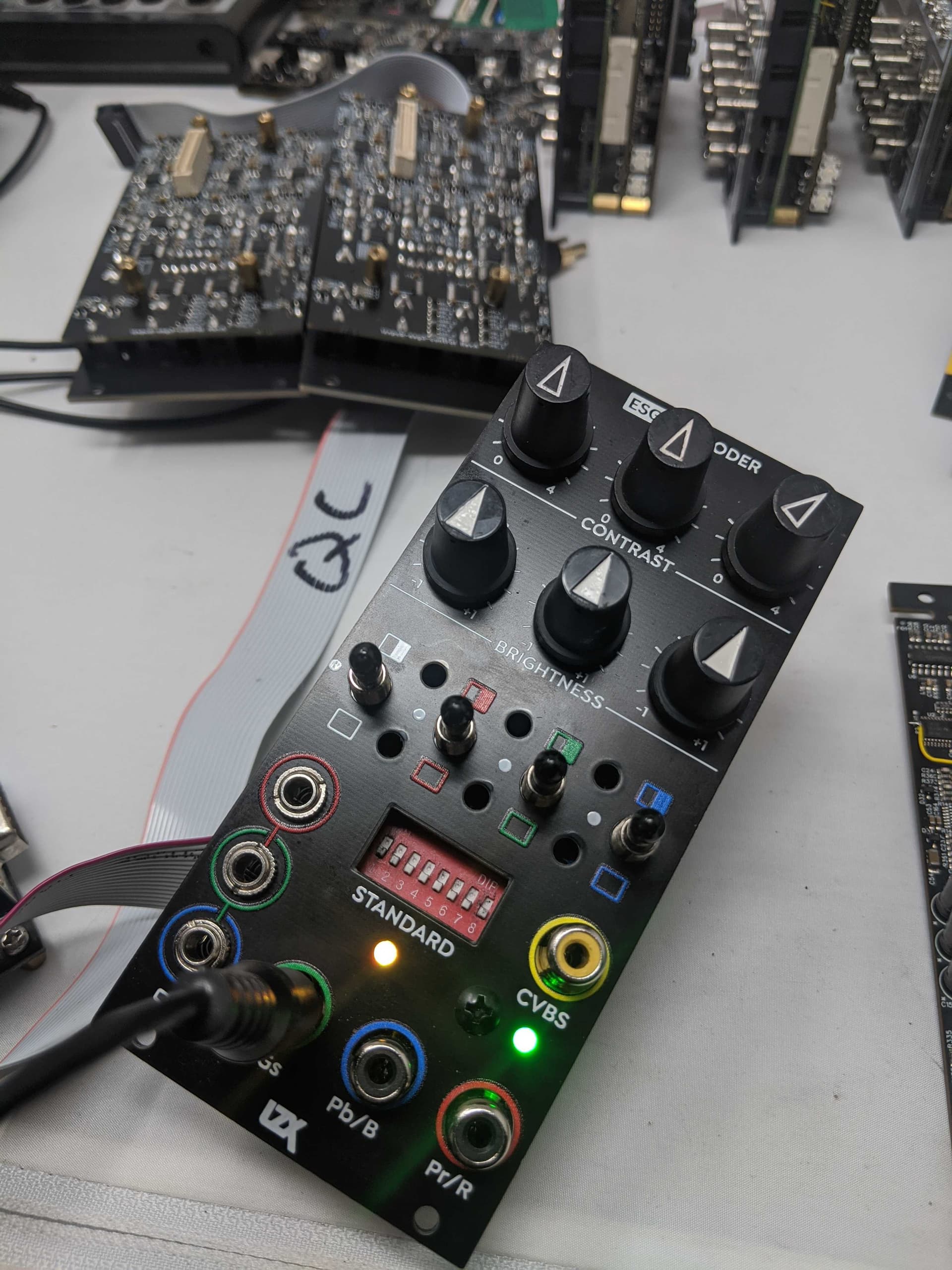
Here’s the earlier esg3 prototype, showing our first approach (which had the FPGA on the core assembly instead of the upper power entry board.)

I hope you enjoyed seeing some process photos, let us know if you want to see more of this kind of thing, and if so, what parts of the process you like seeing most.

30 Likes

I definitely like seeing this kind of thing and hearing about design choices.

If you don’t mind me asking, how come you moved that stuff to the power/sync board? Needed the space on the other board? Or some other reason(s)?

3 Likes

This is a new shared assembly, which means we can maintain the same board for all projects that need HD/SD sync generator and small FPGA capabilities. The big gain is to only be putting an FPGA subsystem on a single board, but use that board in multiple products.

  • power only (lzxpcb-psu8)
  • power + sync input (lzxpcb-sync12)
  • (and this is) power + sync generator w/genlock (lzxpcb-fpga12)

Subassemblies like this make everything more testable and easier to maintain. For exampe, if at some point in the future we need to use a different FPGA part other than the ICE5, we could just revise this PCB while still maintaining pinout compatibility with all the other assemblies that use it.

There are some other benefits too. For example, the esg3-core board is now a more modular analogue output encoder assembly. If in the future we wanted to have two encoders on a single device, we could potentially use two of these assemblies (without having to have redundant FPGAs.)

We had a similar assembly to this in the Visionary series, with the logic modules! The Dual Flip Flops, Logic, and Counter modules all shared a common power + CPLD assembly.

7 Likes

Catchy name! :wink: Always a pleasure getting a look behind the scenes and nerd out over some PCB design

4 Likes

Amazing!
Really interesting to understand the decision making behind and to see in the detail the boards. Thanks for the insights!

5 Likes

I’m always going to enjoy pics like these. Thanks.

3 Likes

Here are some more photos from today.

The ESG3 core PCBA. This board contains 5V/3.3V level shifters, discrete RGB blanking, Component & Composite Video Encoders, an RGB to YUV conversion matrix, and sync combination buffers.

The whole ESG3 assembly. The control board (bottom left) contains the RGB procamp, which uses VCAs and exponential converters. It also contains input buffers, multiplexed RGB inverters and control logic, and some output buffers.

Testing in the light tent is proving highly productive. It makes a nice staging box for the current device under test and any adapters, programmers, or test leads.

18 Likes

Love seeing this stuff, thanks for posting these updates!

3 Likes

Thank you for sharing those photos and letting us be flies on the wall at LZX as you bring these designs to fruition. Personally, I have a new found appreciation for the complexity of the gen3 circuits, at least from the density of the components. I have no intention of disassembling my modules, so I would have never really had the opportunity to see what was going on under the hood. Cheers!

3 Likes

This is a very simple example, but here’s a look at a step in what’s involved with hardware design verification & testing.

After initially powering up an assembly, an important next step is to get 3-5 samples built that are also passing the same tests. We scribble a lot of notes as we go, and use color coded stickers to identify individual boards.

After making sure 5x ESG3 articles (assembled from the three sub-assembly boards) were fully powering up to the same current draws, we can write some simple firmware to verify the FPGA.

Here’s a VHDL snippet showing what some very simple code looks like to increment a counter and use the most significant bits of that register to make the frontpanel LEDs blink.

hdl_snippet

We compiled and programmed the firmware binary onto the FPGA, but nothing happened. It’s very rare that everything works on the first try, though. So the next step was to do some investigation. We traced the LED connections in our schematic through the assemblies, trying to come up with theories about why the LEDs were not blinking yet.

Naturally, the first places to look are places this circuit has changed since it’s last version. That led us to the new level translators on the new version of the core PCBA. Oops! We forgot to add a pullup on this part, which meant the level translator outputs were disabled. No wonder the LEDs weren’t blinking.

Usually we’d dig around for a few more theories before the hardware measurements start, but in this case we were pretty sure this was our issue. We made a quick fix to one board: problem resolved!

Since we got that far, we checked for video output, which was present:

(Homework: Can anyone determine the video format from this scope shot?)

This is an important milestone, since we now know that there is communication across all three PCBs functioning as expected, that our clock generator is running, and that video sync is being generated.

Before getting carried away though, we need to make sure to accurately log our issue and the rework performed in GitHub. This way we’ll have all the notes we’ll need to revise the PCB layout and schematic later, after the review has been completed.

We also make sure we’ve fixed the issue on our other four test assemblies, so fixes can be confirmed multiple times over before we commit to them.

18 Likes

This is all very fascinating to see, thank you for letting us in on the behind the scenes development!

3 Likes

A few end of the week photos. We finished validating the new hardware today. We need to write up some calibration instructions for the workshop team going into next week and run a few more tests, then we’ll be able to sign off on production hardware.

a quartet of video encoders

@eyesnoface calibrating RGB gain/brightness using test ramps


11 Likes

Thanks for sharing details on the hardware/software, being working on my own sync gen, it is super interesting to see!

Also great to see some love for Lattice FPGAs, I started my project using a Xilinx Coolrunner CPLD (as it is used on your older generations of modules iirc), then they are a little small in terms of macrocells/LUTs, so Eric Schlappi convinced me to look into the iCE40. It asks for a few more extra support components (SPI Flash and 1.8V regulator in addition to the 3.3V one), but the UP5K part comes in QFN package (which can be soldered by hand), has about 5K LUTs and is supported by the iCEstorm open source toolchain.

I was tempted using LMH1982 for the clock generator at first, though they’re quite expensive, so went for the PLL+VCXO as shown on Cadet I, looks like that what you’re using here too right? Also, we can see that the flash chip isn’t populated, I presume you’re writing the bitstream directly to the FPGA SRAM?

Hope I’m not annoying with my questions/sharing about my stuff, I’m pretty new to FPGAs and been learning through resources online until now, then this is pretty exciting to see a video sync generator implementation to me!

Here is the board I did, in DIP40 format to be used in DIY projects, with regulators at the top, then sync extractor, PLL+VCXO, iCE40 and finally flash (pardon the poor hand soldering, those tightly spaced 0603 were not super easy to fit). It is greatly inspired by iCEbreaker/UpDuino devboards.

From the time base, we can see that the pulses occurs every ~64us, so would be either 480i or 576i format. Then from the length of the pulses (~10us) we can guess that this is a blanking signal (and the continuous line on the left would be vertical blanking).

14 Likes

Might be the wrong thread to ask, but with the variants involving sync & blackburst, will any of the planned gen3 modules have a sync pass through from front panel to back panel that doesn’t involve burning a camera input? Still eager for a solution to unite front of house and back of house sync throughout multiple cases without needing to DIY, leave a blank space in the rack, or waste a video input.

2 Likes

Might be the wrong thread to ask, but with the variants involving sync & blackburst, will any of the planned gen3 modules have a sync pass through from front panel to back panel that doesn’t involve burning a camera input?

Short answer: Yes. TBC2 has front and rear sync input and output separate from any video IO. That’s the Gen3 module with this feature.

Longer answer: A few utility modules should be added after the launch of the first set (TBC2, Chromagnon, ESG3, DSG3, FKG3, SMX3, DWO3). We’re hesitant to rush into any of them because we want to poll the community after you’ve all spent time patching these. But a general purpose sync/video distribution amplifier, with front and rear IO, seems like a must.

2 Likes

Also great to see some love for Lattice FPGAs

Yes, it has been pretty pain free to work with so far! The form factor is perfect for this use case. Not as fast as the fabric in the Xilinx parts we’ve been using, but so many more resources, smaller package sizes, than something like the CoolRunner CPLDs we used in Fortress/Visual Cortex. We needed a part where we could port our sync gen/timing HDL modules from TBC2/Chromagnon directly and maintain a common codebase, so the CPLD wasn’t going to cut it for this project (but the Zynq much too large/expensive to put on a typical module.) So LP5 has become our “small system” and Zynq our “big system.” The new Zynq board we’ve been working on for Chromagnon is modular too. So an “even bigger system” (like for a future vector-to-raster device) could be realized with multiples of the Zynq board. One of the mistakes with Orion series we made was experimenting with too many embedded system approaches! So I hope we can keep it to just LP5 and Zynq, and some small MCUs, for projects in the foreseeable future.

Also, we can see that the flash chip isn’t populated, I presume you’re writing the bitstream directly to the FPGA SRAM?

Yes, for development we’ve just been writing directly to the CRAM with the Lattice programmer tools. For production the firmware will be written to the Flash, and the part will program from that.

I was tempted using LMH1982 for the clock generator at first, though they’re quite expensive, so went for the PLL+VCXO as shown on Cadet I, looks like that what you’re using here too right? Also, we can see that the flash chip isn’t populated, I presume you’re writing the bitstream directly to the FPGA SRAM?

We’re using the LMH1980 for sync separator and the Cypress 24204 for clock generator. The Cypress part has an integrated 27MHz VCXO but also generates the two HD clocks (74.25MHz and 74.25/1.001MHz). Inside the FPGA we are using the internal PLL to create a 108MHz clock that drives the 3.58MHz and 4.43MHz NTSC/PAL subcarrier generators (FSC clock for AD724 encoder.)

You can read more about the Cypress part here:

Correct! Yes, this is NTSC. You’re actually just seeing the video output itself here, but without any image content.

4 Likes

Right, the iCE serie seems a bit limited to be used for video processing, even more when talking about HD video, though perfect for sync/signal generation purposes. Lattice ECP5 sounds more like a good candidate for this from what Schlappi told me, though it would probably asks for a µC to go with it, so the Zynq serie makes a lot more sense in that case!

That clock generator part is neat! Most of dedicated ICs I found for this were obsolete, and LMH1982 was bit out of the scope in term of price range, so went for the 4046 + 27MHz VCXO route, even though it has some drawbacks such as jitter and resting frequency. Also, I was able to generate a 74.25MHz clock out of the 27MHz VCXO on my board, though 74.25MHz/1.001 couldn’t be achieved with the internal FPGA PLL, so doesn’t allow for 29.97Hz/59.94Hz timings. That’s nice that you can also generate chroma subcarriers from the FPGA, save some board space and cost by not using dedicated crystal oscillators.

Thanks again for the insight on this!

3 Likes

Yeah, the Cypress part is nice. It’s no more expensive than a standalone VCXO+4046 circuit like you’re doing now – we have the VCXO phase comparator inside the RTL on the FPGA. I think we’re going to see more of a low cost market for this particular era of set top box / video encoding IC over the next few years. A lot of the parts that were designed for mass produced SD/HD equipment up to 1080p30 (like this part) are now being deprecated for new devices that use 4K compatible or 1080p60 parts – so there will be excess stock of NOS parts, etc.

Also; another point of putting the FPGA on a subassembly (like we both did!) is that if we need to change the clock generator approach at some point, there are many ways to do that. I would not like having the 24204 on multiple product-specific boards. If we had used a shared assembly with Cadet and Visual Cortex, for example, it would have been easier to update and maintain those designs.

That’s nice that you can also generate chroma subcarriers from the FPGA, save some board space and cost by not using dedicated crystal oscillators.

Yes, and there are some technical advantages to having a subcarrier that is synchronous (PAL “super-frame”) with the sync generator source – it eliminates dot crawl and can result in cleaner analog to digital conversion.

We’ll definitely be working on some DCO engine implementations for this ICE5, and various direct logic functions. I’m not sure what else. It would be interesting to simulate a minimal microcontroller on it, capable of using the SPI or I2C blocks, along with an RTL video function.

4 Likes

I don’t understand the alphabet soup, but it sure is cool to see the progress.

Rock on

This is the kind of post that I know I’ll come back in one year or so and say: aha! All the info I need is here!
Loving it :slight_smile:

2 Likes